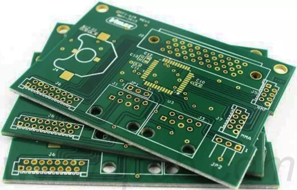
PCB pad is a critical component of printed circuit boards, serving as the interface between electronic components and the circuit board for establishing electrical connections and mechanical support. The quality of pad design directly impacts component soldering reliability, overall product performance, and manufacturing process efficiency.
PCB pad width
The width of the PCB pad should be equal to or slightly greater than (or less than) the width of the solder terminal (or pin).
- Hole diameter size
If the actual pin is circular: Hole diameter size (diameter) = actual pin diameter + 0.2–0.3 mm (8–12 mil);
If the actual size is rectangular: Hole diameter size (diameter) = actual pin diagonal size + 0.1–0.2 mm (4–8); - PCB Pad size: Standard pad size = hole diameter (diameter) + 0.5 mm (20 mil).
- Via size processing: Minimum inner diameter for multilayer boards is 0.2 mm, minimum outer diameter is 0.45 mm; minimum inner diameter for double-sided boards is 0.3 mm, minimum outer diameter is 0.6 mm;
- PCB Pad to board edge distance: >5 mil;
- Minimum character size: line width 6 mil, character height 32 mil;
- Line width/line spacing: 4 mil/4 mil
Calculation formulas as follows:
Pad length B = T + b1 + b2
Pad inner spacing G = L – 2T – 2b1
Pad width A = W + K
Pad outer spacing D = G + 2B.
L — Component length (or distance between the outer sides of the device pins);
W — Component width (or device pin width);
H — Component thickness (or device pin thickness);
B1 — Inner side (pad) protrusion length of the solder point (or pin);
b2 — Outer side (pad) protrusion length of the solder end (or pin);
K — Pad width correction factor.
PCBA Pad Design Standards
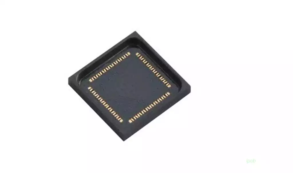
- Fine-pitch IC (0.4 Pitch/0.5 Pitch QFP) Pad Design
Adjacent pads are separated by green solder mask.
Theoretical design: 0.4 pitch IC, pad width 0.2 mm; 0.5 pitch IC, pad width 0.25 mm.
Actual Acceptance: 0.4-pitch IC pad width
- Dip Component Pad Design on Large Copper Areas
Dip components designed on large copper areas should primarily use cross-shaped ring pads on each copper foil layer to reduce heat loss during soldering and improve solderability. (If current is insufficient, the connection width can be increased or a fully exposed copper design can be used.)
If the large copper area is not covered with green paint and not tin-plated, the outer edge of the ring pad must be covered with at least 3mm wide green paint.
- Solder mask width
0.025mm < a < 0.05mm - Chip component pad design
0201 square pad: A = 0.32mm, B = 0.28mm, C = 0.18mm (increase to 0.2mm if space permits)
0402 square pad: A = 0.51mm, B = 0.48mm, C = 0.381mm
0603 Square PAD: A = 0.8 mm, B = 0.76 mm, C = 0.65 mm
0805 Square PAD: A = 1.32 mm, B = 0.8 mm, C = 1.0 mm
1206 Square PAD: A = 1.57 mm, B = 0.97 mm, C = 1.8 mm

Failure caused by incorrect PCB pad dimensions
The dimensions, shape, and position of pads in PCB packaging directly affect the manufacturability of the circuit board. During the soldering process in PCB assembly, using pads with incorrect dimensions or positions may lead to various issues. The following points are listed below:
- Floating components If surface-mount components are placed on pads that are too large or have incorrect spacing, the components may float out of position during reflow soldering. This may cause solder bridges to other metals, leading to thermal cooling, rework, and insufficient component spacing during PCB testing.
- Incomplete solder joints Pads that are too small or spaced too closely may not have sufficient space to form adequate solder balls. This can result in poor solder connections or no solder joints at all.
- Solder bridging Too-large surface mount pads can cause components to float, which may result in solder bridging. This occurs when solder crosses over to another pad or metal feature on the board, creating a direct short circuit. Solder bridging can also occur if the correct solder mask and solder paste features are not designed into the pad shape in the CAD tool.
- Tombstoning Two small fixed SMT components, such as resistors and capacitors, may experience soldering issues if their pad sizes differ. One pad heats up faster than the other, and the melted solder pulls the component upward away from the other pad, causing it to stick like a tombstone.
- Solder wicking Through-hole pads may also encounter issues if constructed improperly. If the drill hole size for the component leads entering the hole is too large, solder may be drawn through the hole core before a good connection is established. On the other hand, a drill bit size that is too small makes inserting the component leads difficult and slows down assembly speed.
- Through-hole open circuit Through-hole pads must have a solid metal ring to ensure solderability, which is the metal between the hole wall and the outer edge of the pad. The ring specifications are designed to be sufficiently large to allow the drill bit to deviate from the hole centre as intended. However, if the pad is too small, the ring may develop some fractures, and excessive fractures can lead to improper soldering or circuit damage and incompleteness. If the pad size is too small for the drill bit being used, the drill bit may slightly wobble and deviate from the pad shape during normal drilling operations.
- Short circuits with other metals A pad that is too small may cause surface traces to come too close to components soldered onto it, creating potential metal short circuit areas. On the other hand, a pad that is too large may restrict trace routing between them, making PCB layout more challenging.
PCB Pad Design and Manufacturing Process Requirements:
- Test points should be added to the ends of surface-mount components that are not connected to through-hole components. The diameter of the test points should be equal to or greater than 1.8 mm to facilitate testing by an in-line tester.
- For IC pads with tight spacing that are not connected to through-hole pads, a test pad must be added. For surface-mount ICs, test points must not be placed within the silk screen of the surface-mount IC. The diameter of the test point must be equal to or greater than 1.8 mm to facilitate testing by an in-line tester.
- If the pad spacing is less than 0.4 mm, white oil must be applied to reduce peak welding.
- The tips and ends of surface-mount components should use lead-tin design. The width of the lead-tin is recommended to use 0.5 mm wire, with a length generally of 2.3 mm.
- If a single-sided board has manually soldered components, a solder slot must be opened. The direction should be opposite to the solder direction. The hole width should be between 0.3mm and 1.0mm.
- The spacing and dimensions of conductive adhesive buttons should match the actual dimensions of the conductive adhesive buttons. The PCB board connected to them should be designed with gold fingers, and the corresponding gold plating thickness should be specified.
PCB pad design is an indispensable part of the electronic product manufacturing process, and its accuracy directly determines the performance and reliability of the product. Adhering to strict design standards and fully considering manufacturing process requirements can effectively avoid welding defects, improve overall production efficiency, and ensure the excellent quality of electronic products.