With the rapid development of science and technology, the impact of digital imaging technology in our lives is becoming more and more profound. From daily smartphones and tablets to high-precision industrial inspection equipment, medical imaging systems, and the drones, smart driving and wearable devices that have emerged in recent years, all kinds of products rely on efficient and stable image acquisition and processing capabilities. One of the key hardware that supports all these operations is the camera circuit board.

The camera circuit board is not only the physical carrier of the image sensor, but also integrates a variety of key functional modules, such as analog signal conversion, digital processing, power management, image optimization, data storage and interface transmission. Its performance, stability, volume and power consumption will directly determine the imaging effect and market competitiveness of the entire camera module and even the terminal product.
In recent years, with the continuous advancement of CMOS image sensor technology, it has achieved a significant improvement in resolution, photosensitivity and low noise performance, making the camera circuit board more integrated, more compact and with a shorter signal link. At the same time, due to the integrated development of emerging technologies such as 5G, AI, and IoT, higher requirements are put forward for the real-time and intelligent performance of the image system, and new challenges are also put forward for the design level of the camera circuit board.
Therefore, in-depth discussion of the core structure, design points, layout and future development trend of camera circuit boards is not only of practical reference significance for electronic engineers, but also of great value for product developers to grasp the cutting-edge technology direction and improve system integration capabilities.
Basic structure of camera circuit board
As the core platform of the image acquisition system, the structural design of the camera circuit board directly affects the image clarity, response speed and overall stability of the system. In order to achieve efficient conversion from optical signals to digital images, a typical camera circuit board usually contains the following core parts: image sensor module, signal processing unit, clock circuit, power management module, data interface and auxiliary function module (such as temperature control, electromagnetic shielding, etc.).
First of all, the image sensor is the soul of the entire circuit board. There are two types of sensors currently used in mainstream applications: CCD (charge coupled device) and CMOS (complementary metal oxide semiconductor). Although CCD has advantages in high sensitivity and low noise performance, CMOS has become the first choice for most consumer and industrial cameras in recent years because it has more advantages in cost, integration and power consumption. The sensor usually needs to be tightly welded or bonded to the PCB board and connected to the image signal processing chip to ensure the integrity and stability of the data transmission process.
Secondly, the signal processing unit is a module used to perform preliminary correction and conversion on the collected raw image data, which often includes processing tasks such as image enhancement, color correction, white balance, and dynamic range adjustment. In high-speed or high-resolution applications, it is also necessary to integrate FPGA or dedicated ISP (image signal processor) chips to provide real-time data processing capabilities.
The clock circuit usually includes a crystal oscillator and a clock generator to provide a stable synchronization signal for the entire image system. If the clock jitter is large, it will cause image offset, blur or synchronization errors, so precise wiring and reasonable layout are required to reduce interference.
The power management module is responsible for powering each chip. Due to the different voltage and current requirements of different modules, the camera circuit board often contains multiple LDOs, DC-DC converters and filter capacitors. In particular, low-noise design should be paid attention to in the power supply part near the image sensor to prevent power ripple from affecting the imaging quality.
In terms of data interface, multiple transmission protocols such as USB, MIPI CSI, LVDS, and HDMI are widely used to achieve data communication with the host system. In consumer products, USB 3.0 has become the mainstream due to its ease of use and high-speed performance; while in high-end industrial or drone scenarios, MIPI and LVDS are widely adopted due to their stronger anti-interference ability and easier onboard integration.
In addition, other auxiliary modules are commonly found in camera circuit boards, such as EEPROM storage modules (to save calibration parameters and sensor ID), temperature sensors (for dynamic gain adjustment), hardware trigger IO (for multi-camera synchronization), and EMI shielding covers and heat sinks added in high-end applications.
An excellent camera circuit board design must strike a balance in structural layout, EMC control, thermal management, space optimization and signal integrity. Structural engineers usually work closely with optical designers and software engineers to ensure that the final product meets both imaging requirements and industrial design standards.
Key design points
In the development process of camera circuit boards, it is not only the selection of components that determines the imaging quality and system performance, but more importantly, reasonable circuit design, precise wiring routing, and efficient thermal management and electromagnetic compatibility (EMC) control. The following are several aspects that must be focused on when designing camera circuit boards:
- Signal integrity design
Since camera circuit boards usually need to process high-frequency, high-speed data transmission signals, such as USB 3.0, MIPI, LVDS and other interfaces, the wiring specifications of high-speed signals must be strictly followed during layout and wiring. For example, when transmitting MIPI data, the signal lines must be kept equal in length and impedance continuous to avoid crosstalk and reflection. In particular, the data lines output by CMOS image sensors are usually located in the center of the board, and the lines between the processing chip should be as short and straight as possible to avoid sharp turns, while considering the return path between different layers.
- Power supply noise control
Image sensors have extremely high requirements for power supply stability. Slight voltage fluctuations or power supply noise will directly affect image quality, resulting in problems such as horizontal stripes, bright spots or color shift. Therefore, low-noise LDO is usually used in power supply design to power the core module, and appropriate filter capacitors and ferrite beads are added to suppress high-frequency interference. Strategies such as partitioned power supply and star wiring should be adopted between different modules to prevent the noise generated by high-power devices from being transmitted to sensitive circuits.
- Heat dissipation management
With the improvement of the computing power of image processing chips, some processors (such as ISP or FPGA) consume high power during operation and generate a lot of heat. If the heat dissipation design is unreasonable, it may cause image blur, module frequency reduction or even system restart. Therefore, when laying out the camera circuit board, the heating components should be placed in a well-ventilated area first, and sufficient copper foil area should be reserved as a heat dissipation path. If necessary, thermal conductive silicone grease, aluminum heat sink, or even active fan should be used.
- Module spacing and size optimization
Due to the requirements of volume and weight, especially in portable terminals such as mobile phones, drones, and wearable devices, camera circuit boards are often required to be as small as possible. How to maximize functions in a limited space is a very typical system engineering problem. Designers need to make full use of the multi-layer board (4-layer, 6-layer or even 8-layer) structure, lay high-frequency signals in the inner layer, tightly couple the power layer and the ground layer, and reasonably divide the analog area and the digital area to avoid mutual interference.
- EMI/EMC design
The camera circuit board is not only affected by external electromagnetic interference, but also may become a source of interference for other circuit systems. Therefore, good EMI design is a necessary condition to ensure system reliability. Common practices include: adding ground protection to key signal lines, differential symmetry of routing, minimizing cross-partition wiring, and using shielding covers to cover sensitive areas. In addition, using a spectrum analyzer for EMI scanning has become a standard process during the system verification phase.
- Optical alignment and mechanical coordination
Although optical and mechanical design seem to be “another world” from a circuit perspective, in camera circuit board projects, the engineering team must consider the coordination of the optical axis position, module height, mounting hole position and the entire machine housing. A common mistake is that the design drawing is reasonable but the module is slightly offset after welding, resulting in dark corners or unclear focus on the edge of the image. Therefore, experienced engineers will design an integrated module bracket or add optical alignment marks on the PCB to ensure assembly accuracy.
In summary, designing a high-performance camera circuit board is not simply piecing together components, but a systematic challenge covering circuits, optics, thermal management and mechanical coordination. Only by striving for perfection in every detail can we create an image module that is truly competitive in the market.
Manufacturing and packaging requirements
A high-quality camera circuit board not only relies on the ingenious design, but also must be accurately realized through high-level manufacturing and packaging processes. Since camera modules involve complex processes such as high-density layout, fine welding, and multi-layer board processing, their manufacturing process requirements are much higher than those of general consumer electronic products. The following is an in-depth analysis of its key manufacturing points from multiple dimensions:
- PCB substrate selection
Camera circuit boards usually use a high-density interconnect (HDI) board structure to support short-distance high-speed communication between image processing chips and image sensors. In terms of substrate selection, in addition to conventional FR-4 materials, high-end applications prefer low-loss, high-heat-resistant materials such as the Rogers series or Panasonic’s Megtron series to ensure stability under high-speed signal transmission.
In some scenarios that need to deal with high temperature or harsh environment (such as industrial inspection, vehicle-mounted cameras), substrates with high TG value (high glass transition temperature) are also used to enhance the thermal stability of the board and prevent deformation, delamination or failure during reflow soldering or long-term high temperature use.
- Circuit processing and aperture accuracy
In order to achieve the goal of high integration and high-density layout in camera circuit boards, the line width and line spacing in the board are often required to reach 50μm or even smaller. This places extremely high demands on the process accuracy of etching, dry film, laser drilling, through-hole electroplating, etc. of PCB manufacturers. In particular, the signal lines and MIPI buses used in CMOS modules usually have very short wiring distances. If there are problems such as etching residues and uneven line width, the signal quality will be directly affected.
In addition, in order to reduce the size of the module, many camera circuit boards use blind buried holes or arbitrary layer interconnection structures. This method can quickly lead the signal from the surface to the bottom of the chip, improving the overall layout efficiency, but it also greatly increases the complexity of board processing. Therefore, manufacturers need to have advanced laser drilling equipment, copper deposition and hole filling capabilities to ensure aperture consistency and conductive reliability.
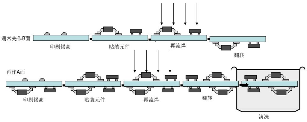
- Welding and mounting technology
Camera circuit boards usually use 0402, 0201 or even smaller package components. The most common core components in the module, such as BGA packaged ISP chips or WLCSP packaged CMOS sensors, have dense and invisible bottom solder joints, and the welding requirements are very high. The entire surface mounting process (SMT) requires the use of high-definition AOI inspection equipment and X-Ray inspection machines to check for solder bridges, empty solder joints or cold solder joints.
Especially in the process of sensor chip mounting, in order to ensure the accuracy of optical alignment, high-precision chip mounters and image-assisted calibration systems are required, and the reflow soldering temperature curve is strictly controlled to avoid component displacement or damage.
- Module packaging form
Depending on different application requirements, the packaging form of camera circuit boards is different. Common packaging solutions include: COB (Chip On Board), COF (Chip On Flex), FPC soft board module, modular plug-in solution, etc.
Among them, COB is a packaging method that directly pastes the image sensor die on the PCB surface and bonds it with gold wire. It has the advantages of low cost and thin thickness, but it has extremely high requirements for the cleanliness of the production environment and the bonding process, and is suitable for large-scale, low-cost consumer products. In contrast, FPC soft board modules can be installed in a curved manner, which is suitable for space-constrained scenarios, such as smart wearable devices, endoscopes and other medical products.
- Assembly yield control
Since camera modules are usually small in size and compact in structure, deviations in any process link may affect the final image performance. Therefore, a strict quality control system must be established from PCB board factories to SMT mounting and then to finished product assembly. By introducing barcode traceability, automated testing, OQC testing, image verification platforms and other methods, the whole process quality traceability and abnormal alarm from components to complete machines can be gradually realized.
For situations where the production yield does not meet the standard, such as the occurrence of problems such as photosensitive area offset, blurred imaging, unstable power supply, etc., it is necessary to cooperate with FMEA failure analysis tools for systematic investigation, and locate the root cause of the problem from multiple aspects such as design source, material batch, and process parameters, and then make improvements.
Application scenarios of camera circuit boards
The flexibility and modular design of camera circuit boards allow them to be widely used in multiple fields. With the rapid development of technologies such as image recognition, artificial intelligence, and intelligent driving, its application boundaries are constantly expanding, and it is becoming the “visual center” of many electronic products.
- Smartphones and tablet devices
Among consumer electronic products, mobile phone camera modules are one of the most typical application scenarios of camera circuit boards. Today’s smartphones are often equipped with multiple cameras, including main cameras, ultra-wide angles, telephotos, and macros. Each module integrates independent CMOS sensors, driver chips, power management units, etc., and its underlying core is a highly integrated camera circuit board. This type of circuit board needs to be extremely small in size, powerful in performance, and support functions such as focus and anti-shake.
- Security monitoring and video doorbells
In home and commercial security systems, from traditional webcams to emerging video doorbells and pan-tilt cameras, camera circuit boards play a key role. These devices usually require high-resolution imaging, infrared night vision, wide dynamic range (WDR) and other features, and also need to transmit images in real time through Wi-Fi, Ethernet and other methods, so they have high requirements for the performance stability and data processing capabilities of the circuit board.
- Unmanned driving and vehicle systems
In the field of autonomous driving, vehicles use multiple cameras to perceive and judge the environment. For example, wide-angle lenses for surround view systems, front-view cameras for pedestrian recognition, and even infrared cameras for monitoring passenger status in the car, all have customized camera circuit boards at their core. These boards not only need to withstand the complex temperature and vibration environment of the car, but also meet the real-time and anti-interference capabilities of image transmission.
- Industrial automation and machine vision
In modern manufacturing, more and more production lines are equipped with visual inspection equipment. The combination of camera circuit boards and industrial lenses can identify the appearance, size, color, etc. of products in real time, and complete tasks such as defect detection, positioning, and grasping. Such systems often require cameras to work stably for a long time, while meeting industrial standards in image acquisition speed and accuracy.
- Medical imaging and diagnostic equipment
In the medical field, portable ultrasound, endoscopes, oral imaging systems and other instruments are increasingly dependent on image acquisition. The camera circuit board in these devices is usually very small and needs to be compatible with high-sensitivity image sensors in low-light environments. For disposable products such as endoscopes, their camera circuit boards often have to take into account cost control and safety and reliability.
- Drones and smart wearables
With the popularity of consumer drones, aerial photography has become one of the entertainment methods for the public. Lightweight, high-performance camera circuit boards enable drones to achieve 4K video recording and image transmission during flight. The same design is also widely used in smart
Wearable terminals such as glasses, head-mounted devices, and smart helmets provide users with first-person video recording functions. As image processing technology continues to evolve, camera circuit boards are playing an increasingly critical role as a bridge between visual hardware and intelligent algorithms. It is not just a substrate that carries components, but also the basis for the performance of modern image systems. From consumer electronics to industrial automation, from medical health to smart travel, its application scenarios are becoming increasingly rich, and technical requirements are constantly upgrading. In the future, with the further integration of artificial intelligence and edge computing, camera circuit boards will continue to evolve towards smaller size, higher performance, and smarter integration.
This small circuit board is quietly shaping the way we see the world.