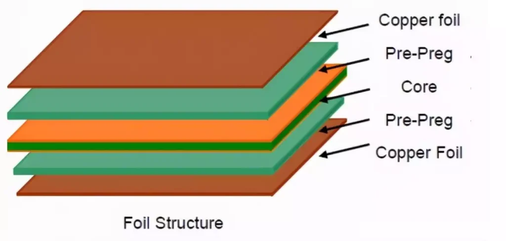
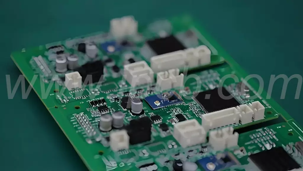
Layers of a pcb is the copper layer, PCB is made of copper layer + substrate compression and become, in addition to a single panel is a layer of copper, double-sided above the board is an even number of pcb layers. Components are soldered on the outermost layer, the other layers play a role in connecting wires, but now there are some high-end PCB will be buried in the PCB components inside the inner layer. PCBs are used in the manufacture of a wide range of electronic devices and machinery in different industries, such as consumer. Automotive. Telecommunications. Aerospace. Military and medical industries. The number of layers and size of a particular board determines the power and capacity of the PCB. As the number of layers increases, so does the functionality.
When selecting PCB design layers, the following key factors need to be considered:
- Application scenario: PCBs are widely used in all types of electronic devices from simple to complex. Therefore, the first task is to clarify whether the application has basic functions or complex functions.
- Signal type requirements: the choice of the layers of a pcb is also affected by the type of signal to be transmitted, including high frequency. Low frequency. Ground or power, etc. For applications that need to handle multiple signals, multilayer PCBs are necessary because these circuits may require different grounding and isolation measures.
- Through-hole type selection: through-hole type is also an important factor to consider when selecting the number of layers. If you choose to bury the type of through-hole, you may need more internal layers to meet the needs of multilayer PCBs.
- Signal layer density and number of requirements: PCB layer determination also depends on the density and number of signal layers. As the pin density decreases, the number of PCB layers required may increase. For example, when the pin density is 1, 2 signal layers may be required.
- Number of Planes Required: The power and ground planes in the PCB help reduce EMI and shield the signal layers. Therefore, the choice of layers also needs to consider the number of planes required.
- Cost control: Although cost control is one of the main requirements,it plays a decisive role in choosing the number of layers for a 1 to 40 layer PCB design. The manufacturing cost of multi-layer PCBs is higher than that of single-layer PCBs, and the cost is highly dependent on all of the above requirements.
- Production cycle time: The production cycle time of a 1 to 40 layer PCB based design is affected by all the above factors. For example,if a design requires only a single layer PCB, the lead time may be shorter.If a PCB is ordered for a complex industrial electronic device,the lead time will be longer.Often,PCB designers will judge the number of layers required based on the complexity of the circuit schematic,which depends on the core devices out of the schematic and the difficulty of the device layout. If a decision cannot be made based on the above factors,it is recommended to communicate with the manufacturer.

Detailed description of the layers of a pcb
- Signal layer (Signal Layers) Altium Designer can provide up to 32 signal layers,including the top layer (Top Layer).Bottom layer (Bottom Layer) and the middle layer (Mid-Layer).The layers can be connected to each other by Via. Blind Via and Buried Via.
(1) The top signal layer (Top Layer),also known as the component layer,is mainly used to place components,for double-layer boards and multilayer boards can be used to arrange the wire or copper cladding.
(2) The bottom signal layer (Bottom Layer),also known as the soldering layer,is mainly used for wiring and soldering, for double-layer boards and multilayer boards can be used to place components.
(3) Middle Signal Layers (Mid-Layers) can be up to 30 layers, in the multilayer board for the layout of the signal lines,which does not include the power lines and ground lines. Signal Layers Signal Layers, that is, PCB printed circuit boards are connected to a variety of alignments.
- Internal power supply layer (Internal Planes) is usually referred to as the internal power layer, only in the multilayer board, the number of PCB board layers generally refers to the signal layer and the internal power layer added to the sum of the number. The same as the signal layer, between the internal electrical layer and the internal electrical layer. Between the internal electrical layer and the signal layer can be through holes, blind holes and buried holes to achieve interconnection. Blind vias and buried vias are used to interconnect the layers.
Blind and buried vias PCB signal layer is the same as the top layer.The signal layer of a PCB is the same copper conductive layer as the top and bottom wiring, but it is the wiring layer sandwiched between the top and bottom layers.Each layer will have a power supply layer.The internal conductive layer (internal power layer) is the internal power and ground layer (and through holes and layers through the layer), the internal power layer design and signal layer wiring is the opposite, because it is negative. Do not draw a line where there is a copper conductive layer, the design of drawing a line where there is no conductive copper layer, this is the difference between them. Internal power layer is mainly used as a shielding ground or power layer,for more than one power supply,it is necessary to split the power layer. Of course, if the wiring is crowded, you can also put part of the power supply alignment in the signal layer, or vice versa, the signal layer of the line in the inner layer.In addition,try to use the internal electrical layer to separate the signal layer,so that the shielding effect is better.
- Silkscreen layer (Silkscreen Layers) a PCB board can have up to 2 silkscreen layer, respectively,the top layer of silkscreen layer (Top Overlay) and the bottom layer of silkscreen layer (Bottom Overlay), generally white, mainly used for placing printed information,such as the outline of the components and labeling, a variety of note characters, etc., to facilitate the PCB component welding and Circuit inspection.
(1) Top screen printing layer (Top Overlay) is used to mark the projected outline of the components.Components of the label.Nominal value or model and a variety of comment characters.
(2) Bottom screen printing layer (Bottom Overlay) and the top layer of the same screen printing layer,if all the marking in the top layer of the screen printing layer have been included,the bottom layer of the screen printing layer can be closed.
- Mechanical layer (Mechanical Layers) mechanical layer, the reason why the emphasis on ‘mechanical’ is that it does not come with electrical properties, generally used to place the production of boards and assembly methods related to the indicative information, such as the PCB form factor. Size marking. Data information. Hole information. Assembly instructions and other information without worrying about any changes to the electrical characteristics of the board. This information varies depending on the requirements of the design company or PCB manufacturer, and the following are examples of common methods.
(1) Mechanical 1: Generally used to draw the border of the PCB as its mechanical shape, so also known as the shape layer.
(2) Mechanical 2: used to place the PCB processing requirements form, including size. Board material. Board layer and other information; for example, Garrigram’s tin slot is set in this layer, see ‘ Summary of the work of the problem of 1) PCB open tin slot ’.
(3) Mechanical 3/4: Mechanical three. Four layers are mostly used to place auxiliary definition of the boundary, as well as special separation lines.
4) Mechanical 5/6: Mechanical five. Six layers are mostly used to place the dimensions of the circuit board.
(5) Mechanical 7/8: Mechanical VII. Eight layers are used to place a variety of descriptive text, such as board number name. Version number. Processing instructions. Designer. Design date and so on.
(6) Mechanical 13 & Mechanical 15: the body size information of most components in the ETM library,including the 3D model of the components; for the sake of simplicity of the page, this layer is not shown by default.
(7) Mechanical 16: the footprint information of most components in the ETM library,which can be used to estimate the PCB size at the early stage of the project; for the sake of simplicity, this layer is not shown by default and the colour is black.
- Masking layer (Mask Layers) Altium Designer provides a soldermask layer (Solder Mask) and solder paste layer (Paste Mask) two types of masking layer (Mask Layers), in which there are top and bottom layers.
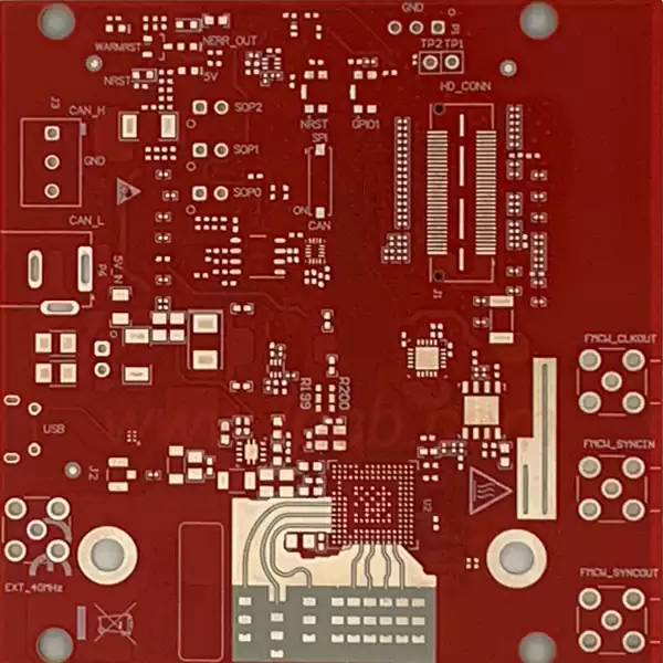
(1) Solder Mask layer is the soldermask layer, is in order to expose the pad with, that is, usually said the green oil layer, the industry is also called open window. In fact, this soldermask layer is used in the negative output,that is,in the green oil layer on the hole, the pads and other places do not need to cover the green oil to reveal the Solder layer is to expose the PAD. In our production package,add Solder Mask layer in the pad, the final production will appear as follows, the golden part is the leakage of the pad, if not open Solder Mask layer,then the pad will be covered by green oil, resulting in we can not carry out the patch. Welding and so on. The following main purpose of this open bare copper is to dissipate heat.The role of the gold finger window: the gold finger window refers to its device pads and pads between the green oil is not on, in order to avoid long-term unplugging and lead to the fallout of the green oil,thus affecting the performance and quality of the product.
(2) Paste Mask layer Paste Mask industry commonly known as ‘stencil’ or ‘steel plate’.This layer does not exist on the printed circuit board, but a separate stencil, above the position of the SMD pad hollow. Generally the cut-outs have the same shape as the SMD pads and are slightly smaller in size. This stencil is used to apply solder paste to the SMD pads in the SMD automatic assembly soldering process.
Paste Mask (solder paste protection layer,SMD patch layer) and the role of the soldermask layer is similar,the difference is in the machine welding corresponding to the surface of the surface paste type components of the pad, respectively,Top Paste (top layer) and Bottom Paste (bottom layer) two solder paste protection layer.Mainly for SMD components on the PCB.If the board is full of DIP (through-hole) components,there is no need to output Gerber files for this layer. SMD components on the PCB board before the SMD pads must be coated with solder paste,in the coating of tin with the stencil must need this Paste Mask file, film film can be processed out.
Paste Mask layer of the Gerber output the most important point to be clear, that is, this layer is mainly for SMD components, Top Paste and Bottom Paste is the top layer. Bottom Pad layer, it is the copper foil that we can see exposed. For example, we drew a wire in the top wiring layer, this wire we see on the PCB is just a line, it is covered by the entire green oil, but we draw a square, or a point on the Top Paste layer at the location of this line, the board played out on this square and this point there is no green oil, but copper foil.
Therefore, the layers of a pcb and structure is the basis of its performance and function, through comprehensive consideration of a variety of factors and careful design, you can create a quality PCB to meet the needs of a variety of electronic devices.


