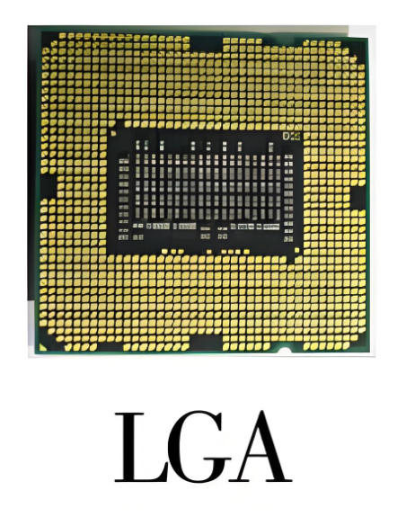
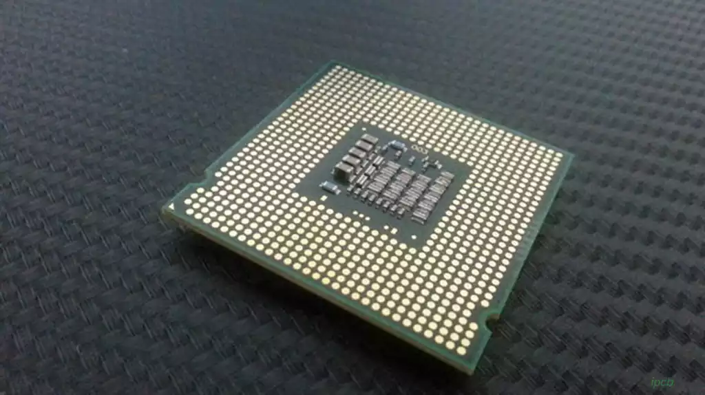
LGA is an electronic component packaging technology based on the Land Grid Array (LGA) connector design principle for connecting IC chips to printed circuit boards (PCBs). LGA is an electronic component packaging technology based on the design principle of Land Grid Array (LGA) connector, which is used to connect IC chips to printed circuit boards (PCBs).LGA package has many advantages, such as high reliability, good heat dissipation, and low insertion and extraction force.
LGA package tutorial
- Prepare materials Before LGA packaging, you need to prepare some necessary materials. These include LGA chips, PCB boards, soldering tools (such as hot air guns or reflow ovens), solder, solder paste, solder wire and so on.
- PCB design First, design the PCB board according to the size and pin arrangement of the LGA chip. Ensure that the pads on the circuit board correspond to the pins of the LGA chip and reasonably layout other components. At the same time, consider factors such as signal integrity and thermal management.
- Attach the pads When attaching the LGA chip to the PCB board, you can use glue or double-sided tape to fix its position for subsequent soldering operations. Ensure that the pins of the LGA chip are accurately aligned with the pads on the PCB.
- Soldering Process a. Use solder paste and soldering flux to apply to the pad locations on the PCB board to increase the stability of the soldering. b. Using a hot air gun or reflow oven, control the temperature and time to melt and connect the solder to the LGA chip and PWB board. c. Pay attention to control the soldering temperature and time to avoid overheating or too long soldering time resulting in component damage.
- Inspection and Testing After completing the soldering, perform a thorough inspection and testing. Ensure that the pins of the LGA package are well connected to the pads, and perform signal testing with test tools to verify solder quality and functionality.
- Troubleshooting If problems are found during inspection and testing, timely troubleshooting is required. Possible causes include poor connection between pads and pins, improper temperature control during the soldering process. Solve the problem by re-soldering or replacing the components.
BGA package (Ball Grid Array Package) is a common packaging technology for electronic components, widely used in the manufacture of modern electronic products.BGA package uses spherical solder joints to connect the chip and the printed circuit board, with high density, reliability and heat dissipation performance. Compared with traditional packaging methods, such as DIP (Dual In-line Package) and QFP (Quad Flat Package), BGA package is more suitable for chips with high integration and high power consumption, especially high-performance integrated circuits, such as microprocessors and graphics chips.
The main feature of the BGA package is a set of tiny metal pads, usually spherical, arranged at the bottom of the chip. These pads are arranged in a uniform grid pattern and are connected to corresponding pads on the printed circuit board. This design allows the BGA package to have a larger number of pins, allowing more pins to be connected in a limited space, resulting in a higher level of integration.
In a BGA package, the chip is connected directly to the pads on the printed circuit board through pads on its bottom.These pads have a larger contact area than in conventional packages, thus providing a better electrical connection and lower resistance. In addition, BGA packages offer better heat dissipation because the solder joints are integrated on the backside of the chip instead of being connected via side pins.
BGA packages also have excellent mechanical strength to resist vibration and shock. Because of the high mechanical stability of the spherical pads, the reliability of BGA packages is important for applications such as mobile devices that require frequent transportation and vibration.
LGA vs BGA
LGA packages are a packaging process that connects to pads on a printed circuit board by soldering contacts. Compared to traditional BGA packages, LGA packages are easier to control the soldering quality during the soldering process because the solder contact points are in direct contact with the pads on the PCB board and do not need to be connected by solder balls, which reduces the number of defective phenomena during the soldering process.
In addition, the LGA package also has better heat dissipation performance, because the solder contact points are in direct contact with the PCB board, the heat is more easily conducted to the PCB board, thus improving the heat dissipation effect. It has been widely used in high-performance integrated circuits, especially in occasions where better heat dissipation performance and solder quality are required.
BGA package is a packaging process that connects to the pads on the PCB board through solder balls. Compared to LGA packages, BGA packages are easier to automate during the soldering process because the solder balls can be accurately soldered by automated equipment, increasing production efficiency.
It also has a higher connection density because the solder balls can be arranged on the entire area on the bottom of the chip, thus increasing the number of connection points, which is suitable for highly integrated integrated circuits. Therefore it is widely used in large-scale integrated circuits, especially where high connection density and automated production are required.
Both LGA vs BGA packaging processes have their own characteristics and advantages, and play an important role in different application areas.