As a core component carrying complex functions and high-density interconnections in modern electronic products, multilayer circuit board faces many technical challenges in the manufacturing process due to their increased thickness, increased number of layers, and dense wiring and perforations. With the increasing demand for high-performance PCBs in fields such as 5G communications, artificial intelligence and automotive electronics, an in-depth understanding of the main difficulties in manufacturing multilayer circuit boards and their solution strategies is of great significance for improving product quality and production efficiency.
Main production difficulties
Compared with the characteristics of conventional circuit boards, high-level multilayer circuit boards have thicker boards. More layers. More dense lines and holes. Larger cell size. Thinner dielectric layer and other characteristics of the inner layer space. Alignment between layers. Impedance control and reliability requirements are more stringent.
- Difficulty of interlayer alignment
Due to the number of layers of the high-level board, customer design side of the PCB layers of the alignment requirements are increasingly stringent, usually inter-layer alignment tolerance control ± 75μm, considering the design of high-level board unit size is larger. Graphics transfer workshop environment temperature and humidity, as well as the inconsistency of different core board layer expansion and contraction brought about by the misalignment of the superposition. Factors such as interlayer positioning mode, making it more difficult to control the interlayer alignment of the high-level board. - Difficulty of inner layer line production
The high-level board adopts high TG, high speed, high frequency. Thick copper. Thin dielectric layer and other special materials, the inner line production and graphic size control put forward high requirements, such as impedance signal transmission integrity, increasing the inner line production difficulties. Line width line spacing is small, more open short circuit, micro-short increase, low pass rate; fine line signal layer is more, the inner layer of AOI leakage rate increases; inner core plate thickness is thin, easy to wrinkle resulting in poor exposure, etching over the machine is easy to roll the plate; most of the high-level board for the system board, the unit size is larger, in the finished product scrapped at a relatively high cost. - Pressing production difficulties
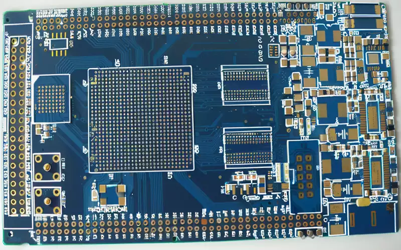
Multiple inner core boards and semi-cured sheet superposition, press production is prone to produce slippery boards. Delamination. Resin voids and air bubbles remain. When designing the laminated structure, it is necessary to fully consider the heat resistance of the material. Voltage resistance. When designing the laminated structure, it is necessary to fully consider the heat resistance of the material, the voltage resistance, the amount of glue filling and the thickness of the medium, and to set a reasonable program for pressing the high-level board. The number of layers, shrinkage control and size coefficient compensation can not maintain consistency; interlayer insulation layer is thin, easily lead to interlayer reliability test failure. Figure 1 is a defective diagram of burst board delamination after thermal stress test. - Drilling production difficulties
The use of high TG. high speed. high frequency . Thick copper special plates, increased drilling roughness. Difficulty of drilling burrs and removing drilling dirt. More layers, cumulative total copper thickness and plate thickness, drilling easy to break the knife; dense BGA, narrow hole wall spacing caused by CAF failure; due to the thickness of the plate is easy to lead to the problem of oblique drilling. - Material selection
High-frequency boards have low requirements for the material’s dielectric constant and dielectric loss, while also requiring low CTE. low water absorption and better high-performance copper-clad materials to meet the processing and reliability requirements. - Thermal management issues
High multilayer circuit board due to the number of layers, heat dissipation is more difficult, need to pay special attention to thermal design and management. - Signal integrity and electromagnetic compatibility
High multilayer circuit board needs to realize better signal integrity and electromagnetic compatibility, which requires full consideration of signal transmission paths and shielding measures during design. - Impedance Control
For high-frequency signals, impedance control is particularly important, requiring precise control of the parameters of the alignment and dielectric layers to ensure the quality of signal transmission.
Multilayer circuit board manufacturing difficulties in the solution strategy
- Enhance the professional skills and practical experience of designers
Enhance the professional skills and practical experience of designers by strengthening the training and technical exchanges of the design team, so that they can effectively cope with the challenges of complex multilayer circuit board design. At the same time, actively introduce advanced design software and tools to improve design efficiency and accuracy. Ensure that designers strictly comply with industry manufacturing specifications and PCB manufacturers’ process capability standards, so as to meet the manufacturing requirements of most PCB production plants. - rigorous control of material quality and process parameters
Meticulous screening and quality control of all raw materials used to ensure that their performance meets strict standards. Meanwhile, the management of production process parameters is strengthened to ensure the stability and quality reliability of each process. Through the introduction of high-end testing equipment and perfect quality management system, such as the expansion coefficient of the sheet. Through the introduction of high-end testing equipment and perfect quality management system, we carry out actual tests on key indexes such as the expansion coefficient of the sheet, the change of film size, etc., and analyze the data of different brands of materials. A database is established and regularly reviewed to ensure that the raw material parameters continue to meet the requirements. - Optimize the inner layer production process
Adopt high-precision line production equipment and high-quality materials, such as laser direct imaging (LDI) exposure machine. Vacuum etching machine and plasma etching machine, etc., to improve the fineness and consistency of the line pattern. Regular calibration and maintenance of high-precision equipment to ensure the stable performance of manufacturing equipment. In the interlayer connection process, the use of high-temperature melt semi-cured sheet (PP) and conductive adhesive and other technologies to ensure the stability of the interlayer electrical connection and mechanical bonding. The connection process is strictly controlled in terms of temperature, time and pressure to prevent material and structural damage. Time and pressure to prevent adverse effects on the material and structure. At the same time, strengthen the quality control of all aspects of the production of the inner layer to ensure that the material and process meet the design requirements. - Reduce the alignment error between layers
Utilize high precision cutting tools. Automatic alignment and advanced laminating equipment to ensure that the dimensions and positions of each layer are highly accurate, thus improving the inter-layer alignment accuracy. Through advanced design and simulation software, predict and adjust the inter-layer deviation before production, so as to enhance the manufacturing quality and reliability of products. At the same time, a perfect quality inspection and control system is constructed to monitor and inspect each process in real time to ensure that the material and process of each layer meets the requirements and significantly improves the interlayer alignment. - Enhance the outer layer production and surface treatment process.
Selection of high-precision drilling equipment. Copper sinking and plating process to ensure the thickness of copper holes in the line manufacturing. Surface copper thickness. Line width, line spacing and etching accuracy meet the design specifications. Strictly control the surface treatment process, such as tin spraying. OSP (Organic Protective Sheet), etc. to improve soldering performance and appearance quality. Precise control of chemical composition, temperature and time parameters during surface treatment to ensure the quality of treatment. Temperature and time parameters are precisely controlled during the surface treatment process to ensure the quality and stability of the treatment. Introducing advanced optical inspection technologies and visual recognition systems for online real-time monitoring of outer layer production to ensure consistent and stable product quality. These technologies are often developed in collaboration with inspection equipment manufacturers or in-house.
Multilayer circuit board manufacturing faces many complex challenges, but by improving design strength, strict material control, optimizing process flow and strengthening inspection methods, these difficulties can be effectively resolved to ensure product quality and performance to meet the needs of high-end electronic applications.