Mobile pcb refers to printed circuit boards used in mobile devices (e.g., cell phones, tablets, portable chargers, etc.). Such boards are usually designed to be thin and lightweight and efficient, capable of supporting high-density arrangements of multiple electronic components to meet the miniaturization requirements of the devices.
Mobile PCB primarily uses a variety of materials, which are usually selected based on different application environments and performance requirements. These materials include FR-4, polyimide (PI), metal substrates, ceramic substrates, and CEM-1/3. Proper selection of board materials is critical because it directly affects board performance, reliability and cost.
1.FR-4
FR-4 is the most commonly used circuit board material and its main components are glass fiber and epoxy resin. It has good insulating properties, mechanical strength and temperature resistance, and is widely used in the manufacture of electronic products.FR-4 is able to meet the needs of most common electronic devices, such as computers and communication equipment.
2.Polyimide (PI)
Polyimide is a high performance flexible material for applications requiring high temperature and high frequency. The material can operate in environments up to 400°C and has excellent mechanical, electrical and thermal properties. Polyimide is widely used in mobile devices such as cell phones and tablets, especially in designs that require flexing and light weight.
3.Metal Substrates
Metal substrates usually use aluminum or copper as the base material and have excellent thermal performance for high power and high temperature applications. These PCB boards are often used in power-intensive applications such as LED lighting, power amplifiers,etc. to ensure the stability and reliability of electronic devices when operating at high power.
4.Ceramic Substrate
Ceramic substrate is a PCB material for high-temperature, high-frequency and high-speed applications with good thermal conductivity and dielectric properties. This material is commonly used in microwave circuits and high-frequency applications, and performs particularly well in high-temperature environments, making it suitable for devices with extremely high signal integrity requirements.
5.CEM-1/3
CEM-1 and CEM-3 are composite substrates made of glass fiber and paper with high temperature performance and cost-effectiveness, and are commonly used in low-end and mid-range electronics. They are suitable for the production of single- and double-sided circuit boards for application scenarios that do not require high performance, such as some everyday electronics.
Factors to consider when selecting materials for mobile pcb:
1.Dielectric constant (Dk)
Dielectric constant (Dk) is an important indicator for evaluating the electrical properties of circuit board materials. It is used to characterize a material’s ability to store and propagate electromagnetic signals. A lower Dk value usually means faster signal propagation with less delay, which is especially important for millimeter wave circuits such as 77 GHz automotive radar systems.
2.Loss Factor (Df)
The loss factor (Df), or dissipation factor, is a measure of the energy loss in a material. A lower Df value reduces the energy loss of the signal during transmission, thus improving the overall efficiency of the circuit. For higher frequency applications, it is critical to control Df values in the lower range to ensure signal quality and system performance.
3.Thermal Properties
Thermal properties include the glass transition temperature (Tg) and the thermal conductivity of the material. tg is the temperature at which the PCB changes from a hardened state to a softened state under thermal stress, and a higher tg can help improve the stability of the material in high temperature environments. In addition, good thermal conductivity can effectively reduce the operating temperature of the circuit board to prevent performance degradation caused by overheating.
4.Moisture absorption rate
Moisture absorption refers to the ability of the material to absorb moisture, the lower the value is more conducive to high-frequency applications. High moisture absorption rate may lead to fluctuations in material performance, affecting circuit stability. When selecting PCB materials, it is often desirable to keep this value between 0.1% and 0.2% to ensure reliability.
The layout of mobile pcb is an important part of ensuring that circuits work properly, improving performance and reducing interference. Reasonable layout can not only shorten the signal path, optimize the power supply and grounding design, but also enhance the reliability of the circuit board:
1.Layout principles
Layout should follow the “first big and then small, first difficult and then easy” principle, that is, the important unit circuits and core components should be prioritized. This method can more effectively use the board space, and reduce potential interference. In addition,complex circuit modules should be the first to complete the integrated design to ensure that the arrangement of subsequent components will not affect its performance.
2.Minimize wire length
One of the keys to realizing a mobile pcb layout is to minimize the length of connecting lines, especially critical signal lines.Shorter wiring not only reduces signal delay, but also reduces signal interference.Therefore,when wiring, priority should be given to arranging signal lines in shorter spaces and ensuring that power and ground lines are arranged logically and clearly,which helps to reduce inductance and resistance.
3.Separation of signal and power supply
High-voltage, high-current signals and low-voltage weak signals should be completely separated from the layout to avoid signal interference and crosstalk. When designing mobile pcb,it should be ensured that analog signals, digital signals, and high-frequency signals are isolated from each other. This can effectively reduce electromagnetic interference and ensure the stability and reliability of signal transmission.
4.Decoupling capacitor layout
Decoupling capacitors in the layout should be arranged as close as possible to the power supply pins to improve power stability and reduce noise. If the decoupling capacitor and power supply pins between the alignment path is too long, will increase the inductance of the power supply, thus affecting the performance. Therefore, it should be ensured that the connection between the decoupling capacitor and the power supply is short and straight.
5.Hole and Component Layout
When laying out the circuit, attention should be paid to the distance between the vias and components to avoid short circuits and signal interference.Especially in high-frequency design, the layout of vias needs to be minimized.In addition,it should be ensured that the power supply pins and grounding holes are properly arranged to minimize interference and problems that may be encountered during soldering.
6.Arrangement of signal lines
Reasonable signal line arrangement is also a key factor affecting the performance of the board.In wiring,should avoid the signal lines of the cross and interfere with each other, try to maintain the balance of the signal lines,and control the spacing between adjacent lines to reduce crosstalk.If it is necessary to lay signal wires in parallel, consider using ground or power lines to separate them to achieve a good shielding effect.
Manufacturing process of mobile pcb:
1.Design phase
The design and manufacturing phase is the first step of the entire PCB fabrication process.During this phase,engineers will design PCB layouts using CAD software and convert them into production file formats for subsequent manufacturing.This process requires precise planning to ensure the performance and functionality of the board.
2.Material Preparation
Choosing the right material is critical in mobile PCB manufacturing.Commonly used substrate materials include FR-4 (glass fiber reinforced epoxy resin), PTFE (Teflon), etc. These materials have good electrical properties and mechanical strength. The choice of material directly affects the performance and application areas of the circuit board.
3.Printed Circuits
Printed circuits use a special printing technique to form a circuit pattern on a substrate. In this process, the circuit pattern is first transferred to a photosensitive coating, which is then hardened by UV exposure, leaving the desired conductive path.
4.Copper Plating and Etching
After the printed circuit is completed, the board is copper plated to thicken the copper layer on the circuit.Excess copper is then removed through an etching process to create a complete circuit pattern.This process requires precise control to ensure the high quality and reliability of the circuit.
5.Drilling
Drilling is the step used to create component pin insertion holes and through holes.The technician places the board into a device called an optical piercer to ensure that each hole is positioned exactly where it should be.This step plays an important role in the assembly and performance of the board.
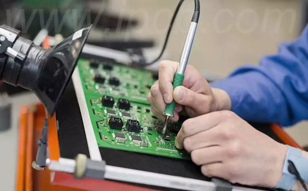
6.Assembly and Testing
During the assembly stage,components are mounted onto the printed circuit board,usually using surface mount technology (SMT) or through-hole technology. Once assembly is complete,the board is thoroughly tested for functionality to ensure that it meets design requirements and performance standards.
The design and manufacture of mobile pcb is critical to modern electronic devices.Through proper material selection, layout optimization and precise manufacturing processes,we are able to ensure that the boards operate efficiently and reliably.As technology advances, continuous updating of design concepts and the use of new materials will be the key to meeting the challenges of the future. This will help to enhance product competitiveness and provide users with a superior experience.