MSAP is an acronym for Modified semi-addition process (MSAP) technology, a processing method for printed circuit boards. The method is mainly through the formation of blind vias between the two layers of the board, making the board more compact, thus realizing the wiring in a smaller space. And blind buried holes such process is an important element in the MSAP process, which not only speeds up manufacturing, but also makes the board more reliable.
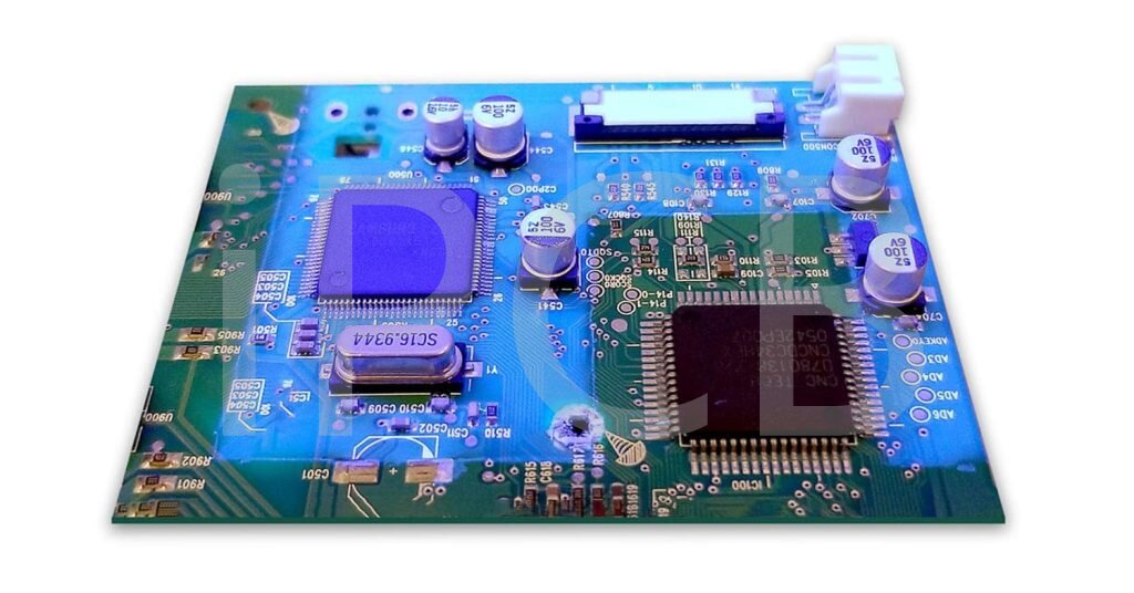
The core of the MSAP process lies in the manufacturing and soldering assembly of microvia. Microvias are tiny holes in a pcb substrate, usually at the micron level in diameter. These microvias form electrical connections between the upper and lower layers of the circuit board, allowing electronic signals to travel smoothly.
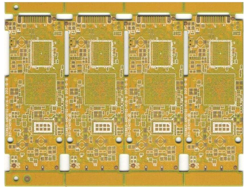
The processing of microvias is a critical step in the MSAP process. Commonly used processing methods include laser drilling and mechanical drilling. Laser drilling utilizes a high-energy laser beam to accurately punch holes in the PCB plate with high precision and efficiency. Mechanical drilling, on the other hand, uses equipment such as drills and drilling machines to physically punch holes in the PWB. Regardless of which method is used, the diameter, depth and positional accuracy of the holes need to be strictly controlled to ensure soldering quality and electrical performance.
After completing the microvia processing, the next step is the soldering assembly step. Soldering is usually performed using surface mount technology (SMT). In this process, components are precisely placed at specified locations on the circuit board and then connected to the microvias on the PWB by soldering equipment. The soldering process requires strict control of parameters such as soldering temperature, time and pressure to ensure the quality and reliability of the solder joints.

Advantages of mSAP technology
MSAP technology saves space by allowing a denser layout of conductive paths. This opens the way for miniaturization of printed circuit boards and devices.
Short signal paths improve signal transmission on printed circuit boards.
Higher performance can be achieved in smaller sizes.
Provides ultra-thin printed circuit boards for ultra-thin devices.
Makes printed circuit boards smaller to make room for sensors, cameras and larger batteries.
The msap process, an advanced printed circuit board manufacturing technology, provides a high-precision, high-density connection solution for modern electronic devices. Through the processing of microvias and soldering assembly, the electrical connection between components is realized, which improves the performance and reliability of electronic devices.