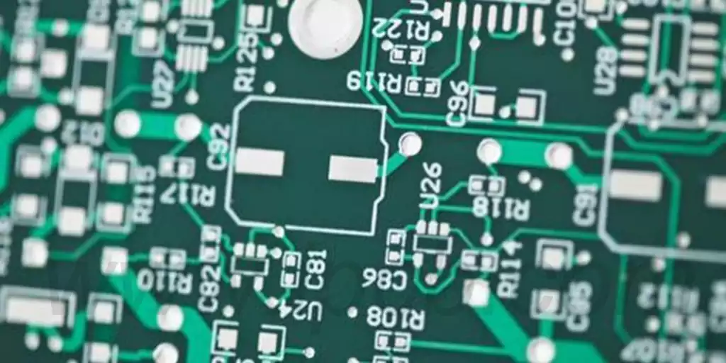
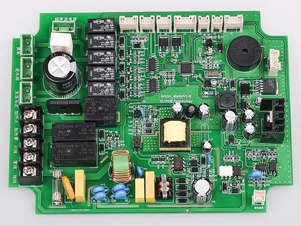
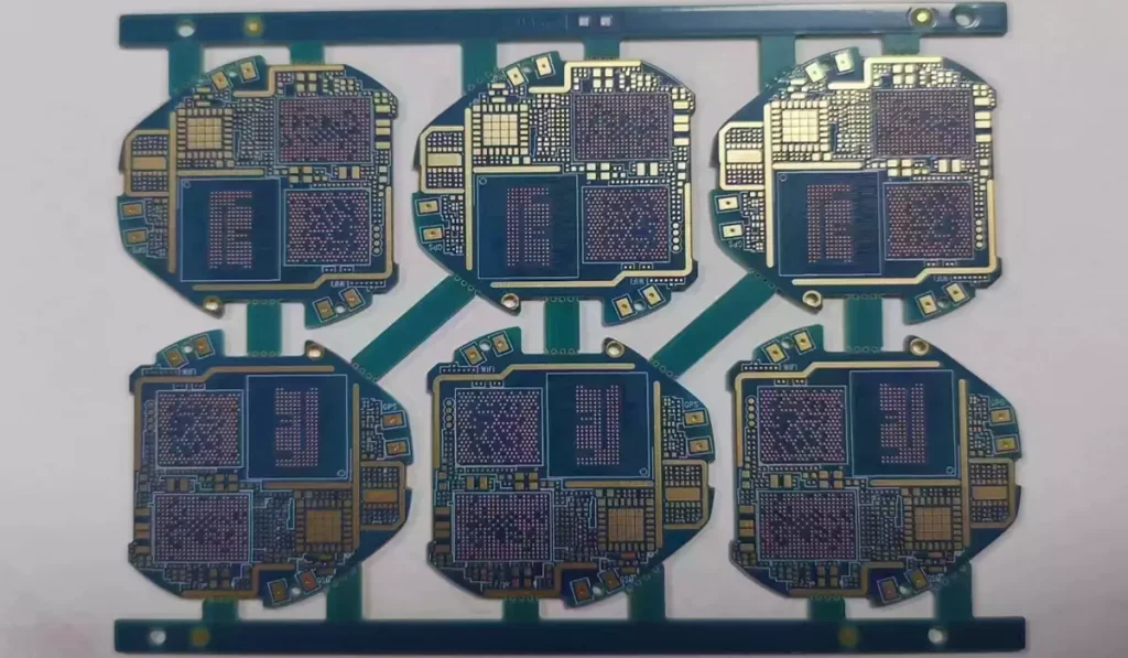
Multilayer PCB, also known as a multilayer circuit board, is a printed circuit board consisting of multiple layers of conductive graphics and insulating materials. These pcb boards have multiple conductive layers, usually isolated from each other by insulating materials. Multilayer pcb is widely used in the manufacture of electronic products for their flexible design, stable and reliable electrical performance, and superior economic performance.
In multilayer PCB, the conductive patterns of each layer are connected through conductive vias to realize circuit connectivity. Since multilayer PCB boards have more wiring space and higher assembly density, they can realize more complex circuit designs and higher reliability. In addition,it has better heat dissipation and electromagnetic shielding performance, which can meet a variety of different application requirements.
The fabrication process mainly includes the following steps:
Design and pre-treatment: before making a multilayer printed circuit board, a detailed design is required to determine the layout of the board, the number of layers, conductive materials, insulating materials, and so on. At the same time, the substrate needs to be pre-treated, such as cleaning and drying.
Make the inner layer of the circuit: According to the design drawings, make the circuits and conductive holes in the inner layer of the multilayer board. This step can be accomplished by photolithography, etching, plating, and other methods.
Bonding: The pre-treated inner layer circuit boards are bonded together by adhesives to form a whole multilayer printed circuit board.
Drilling and Hole Metallization: Drill holes in the multilayer printed circuit board and deposit metal on the walls of the holes to achieve conduction between different layers. This step can be accomplished by mechanical drilling, laser drilling, and other methods.
Outer layer circuit production: the outer layer of the multilayer PCB has been completed in the production of the inner layer of the circuit production of the outer layer of the production of the circuit, can be completed using photolithography, etching, plating, and other methods.
Surface treatment: protection and enhancement of the surface of the multilayer PCB, such as coating, spraying, and so on.
Testing and Inspection: Testing and inspection of the fabricated multilayer PCBs to ensure that their performance meets the requirements.
The differences between multilayer PCB vs single PCB are as follows:
Structure: A multilayer PCB board consists of three or more layers of circuit boards stacked on top of each other, and the connectivity of the circuits is realized through the conductive holes. Single panel only one side of the conductive lines, the other side is blank.
Production methods: The multilayer PCB board production process is complex, needs to go through several punched holes and lamination, while the single panel only need to make a good conductive line on a single side.
Circuit density: the circuit density of the multilayer PCB board is higher, because more circuits can be arranged in a limited space, more suitable for the design of highly integrated products. The circuitry of single-sided boards is relatively simple and is suitable for simpler circuit designs.
Cost: The production cost of multilayer PCB is higher because the production process is complicated and requires high-precision equipment and specialized technicians. The cost of single layer PCB board is relatively low and is suitable for products with less demanding circuitry.
Reliability: The reliability of multilayer PCB is higher because their structure is more stable, able to withstand greater mechanical and thermal stresses, and less prone to deformation and fracture and other problems. The reliability of single PCB is relatively low because their structure is simple and easily affected by the external environment.
Multilayer PCB material requirements include the following aspects:
Substrate material: The substrate material for multilayer PCB is generally FR-4 or aluminum substrate, and different materials are selected according to different needs.FR-4 has good heat resistance, electrical properties, and processing performance, and is one of the most commonly used substrates. Aluminum substrate has the advantages of lightweight, good thermal conductivity, high strength, etc., and is suitable for special applications.
Conductor: The conductor material is generally copper because copper has excellent electrical conductivity and processability. The number of conductor layers in a multilayer PCB depends on the design requirements and is generally 2-8 layers.
Insulating layer: the insulating layer material is generally polyimide, polyester epoxy resin, etc., these materials have good insulation properties, heat resistance, and processability. The thickness of the insulating layer is generally based on design requirements, generally tens to hundreds of microns.
Covering layer: the covering layer material is generally epoxy resin or polyimide, etc., these materials have good heat resistance, electrical properties, and protective properties. The role of the cover layer is to protect the circuit board from environmental influences and mechanical damage.
Adhesive layer: multilayer PCB between the layers need to be bonded with an adhesive layer, adhesive layer materials are generally epoxy resin or polyimide, etc. The role of the adhesive layer is to ensure the structural stability and reliability of the multilayer PCB.
Advantages mainly include the following aspects:
High integration: multilayer PCB can be arranged in a limited space with more components and lines, improving the integration of the circuit, which is conducive to the realization of more complex circuit design.
Excellent electrical performance: multilayer PCB have high conductivity and low resistance, which can provide stable electrical connections and high-speed signal transmission.
Good thermal performance: the multi-layer design of multilayer PCB is conducive to heat dissipation, which can reduce the operating temperature of electronic products, and improve their stability and reliability.
Cost savings: Multilayer PCB can reduce unit costs in mass production and can reduce the number of connected wiring harnesses, further simplifying the assembly and maintenance process.
However, there are also some disadvantages:
High design and manufacturing multilayer PCB costs: the design and manufacturing process of multilayer pcb is more complex, requiring high-precision equipment and specialized technicians, and therefore more costly.
Difficulty in modification: Once the design of a multilayer printed circuit board is finalized, it is more difficult to modify it at a later stage, and it may need to be re-designed and remanufactured, which increases the cost and time of research and development.
Reliability problems: The high density of components and circuits in multilayer PCB is easily affected by the environment, such as temperature and humidity, which may lead to reliability problems.
Multilayer PCB is an important electronic component whose design and PCB manufacturing process requires a high degree of specialized knowledge and technology. With the continuous development of electronic technology, the application areas of multilayer PCB board will continue to expand, and the demand for high performance, high reliability, and miniaturization will continue to increase.