Multilayer PCB stackup technology, in short, is the process of stacking multiple circuit board layers together through specific connections to form a circuit board structure with higher integration and more complex functionality. By increasing the number of circuit board layers, this technology allows more electronic components and circuits to be accommodated in a limited space, thus improving the overall performance of the electronic device.
Basics of multilayer pcb stackup design
①Interlayer Connections
In the multilayer PCB board stacking design, the interlayer connection is very critical, which can be realized by setting up connection holes between layers or through the inner layer connection, in the design process, the reliability of the connection should be fully considered, the cost and manufacturing difficulties.
② Power Distribution
Power distribution is an important part of stacking design. In order to provide a stable power supply, the power supply layer is usually designed in the middle of the multilayer board, through which the power can be distributed to each layer through connection holes in the vertical direction.
Advanced fundamentals of multilayer board stacking design
①Consider signal integrity
When designing, it is important to minimize the length of the signal path as much as possible as a way to reduce signal interference and reflections, and it is also important to choose appropriate line widths and line spacing to prevent signal crosstalk;
② Consider power integrity
To ensure a stable power supply, the power supply layer should be designed in the middle of the PCB multilayer board and connected to each layer through the connection holes, in addition, appropriate decoupling capacitors should be selected to reduce power supply noise and voltage transients;
③Consider thermal design
If the heat dissipation design, you can set up heat dissipation holes in the PCB board, the use of heat sinks or heat-conducting materials and other methods to improve the thermal performance of the device, in addition, should choose low-power components and circuit design, as a way to reduce the total heat generated by the device.
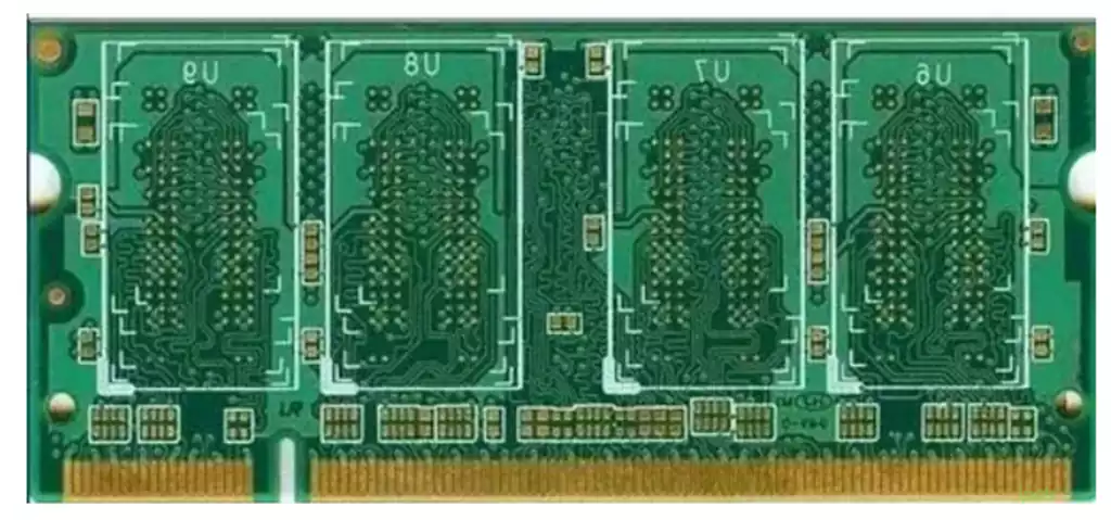
Basic Structure of Multilayer PCB
Multi-layer PCB boards are constructed by alternately stacking multiple layers of conductive material (usually copper foil) and insulating material (e.g. FR4). By drilling holes between these layers and filling them with conductive material, it is possible to form conductive paths connecting the different layers, the so-called “via” (via). This design allows circuits to be laid out in three dimensions, greatly increasing the wiring density.
Multilayer PCB Stacking Design
Stacking design for 4-layer boards:
1.sig 01-gnd 02-pwr 03-sig 04
2.sig 01-pwr 02-gnd 03-sig 04
3.PWR 01-SIG 02-GND 03-SIG 04
Option 1: Usually applied when the main components are laid out on the top or the key signals are wired on the top, better SI performance can be obtained. It is not very good for EMI performance, but it can be controlled by alignment and other details.
Option 2: Similar to Option 1, applicable to the case where the main components are laid out on the bottom or key signals are wired on the bottom.
Program 3: the power supply and ground plane are placed on the top and bottom layers, can achieve a certain shielding effect. However, affected by the power supply and ground layer too far apart, component pads and other factors, the power supply layer and ground layer lack of effective coupling.
Program one and program two compared to program one is more appropriate because the general circuit boards are only placed in the top layer of components. Program three drawbacks are obvious, should not be used.
Stacking design for 6-layer boards:
- SIG 01-GND 02-SIG 03-SIG 04-PWR 05-SIG 06
2.SIG 01-SIG 02-GND 03-PWR 04-SIG 05-SIG 06
3.sig 01-gnd 02-sig 03-pwr 04-gnd 05-sig 06
Option 1: has more signal layers, which is good for the wiring work between components. Disadvantages: ① power and ground layers are far apart and not fully coupled, ② SIG 03 and SIG 04 signal layers are directly adjacent to each other, easy to crosstalk.
Option 2: Compared to option 1, the power and ground layers are fully coupled, but the SIG 03 and SIG 04 signal layers are directly adjacent to each other, so the problem of easy crosstalk has not been solved.
Scheme III: The power and ground layers are fully coupled, and each signal layer is directly adjacent to the internal electrical layer, which can be effectively isolated from other signal layers, and crosstalk is not easy to occur.
In summary, the advantages of Program III is more obvious, but also 6-layer board commonly used layer stacking structure.
Stacking design for 8-layer boards:
- SIG 01-GND 02-SIG 03-GND 04-PWR 05-SIG 06-GND 07- SIG08
2.SIG 01-GND 02-SIG 03-PWR 04-GND 05-SIG 06-PWR 07- SIG08
3.sig 01-gnd 02-sig 03-sig 04-pwr 05-sig 06-gnd 07- sig08 SIG08
For 8-layer boards, Option 1 is prioritized to effectively reduce the power supply impedance and includes two wiring layers, which greatly improves the quality of the signal.
In terms of the basic structure and stacking design of multilayer PCB boards, different layer numbers and design strategies have a direct impact on the performance of the board. Through reasonable multilayer pcb stackup design, the power supply and ground layer can be fully coupled to optimize the layout of the signal layer, reduce signal interference, and improve the stability of the power supply. Therefore, in practical applications, it is crucial to select an appropriate stacked layer design scheme according to specific requirements and constraints.