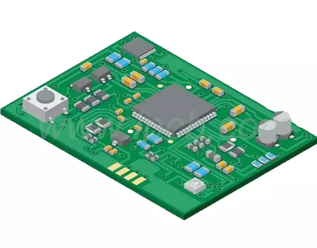
A radio frequency circuit board (RF PCB) is a type of circuit board specifically designed to handle high frequency and radio frequency signals. Compared to ordinary PCBs, RF PCBs have unique design requirements for efficient signal transmission in the high frequency range. Impedance matching and signal integrity are important in RF circuit board design and require the use of special materials such as PTFE (Polytetrafluoroethylene) and Rogers, which have low dielectric loss and high thermal stability.
Multilayer rf pcb design alignment ules:
Impedance control is a core principle in RF PCB design. Typically, RF circuits have a characteristic impedance of 50 ohms, which helps to maximise power transfer and reduce signal reflection. Impedance mismatch can lead to signal distortion, increased losses and EMI problems. Impedance matching can be achieved by selecting the proper alignment width, thickness, and distance between the alignment and the grounding layer, which need to be calculated based on the characteristics of the PCB material and the frequency being operated.
The length and width of the alignment will directly affect the transmission characteristics of the signal. The width of the alignment should match the frequency of the signal and the required characteristic impedance. An excessively long alignment may result in signal attenuation and time delay differences, while an inappropriate alignment width may result in impedance discontinuities. During design, the length of the alignment should be minimised and the appropriate alignment width should be selected according to the frequency and PCB material properties.
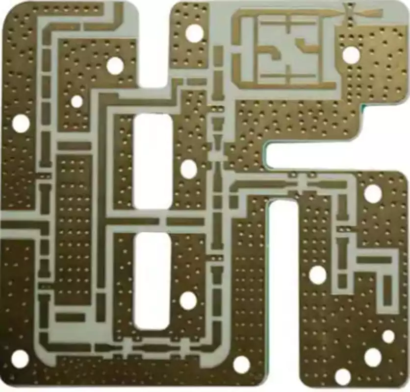
The RF alignment should be on the outer layer of the PCB as much as possible in order to form a microstrip line structure, which helps to better control the impedance. When the alignments must be on the inner layer, make sure they are surrounded by a grounding layer to form a stripline structure to reduce crosstalk and radiation.
For RF devices with antennas, the design of the antenna and the way it is fed can have a significant impact on system performance. The length of the antenna, the feed point and the design of the grounding layer need to be carefully considered to ensure efficient signal radiation and reception.
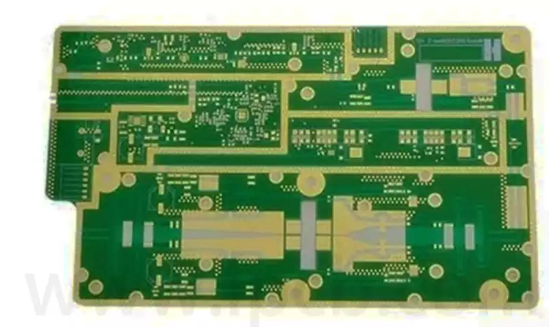
The design of RF multilayer boards is more complex compared to the design of ordinary multilayer boards, mainly in the following aspects:
- signal integrity issues: RF signals are affected by the environment inside and outside the board, prone to crosstalk, reflection, attenuation and other issues, a series of measures need to be taken to ensure signal integrity.
- material selection issues: RF multilayer board material selection needs to be considered inside and outside the board dielectric constant, loss and other factors, the need to choose high-performance materials.
- Layout and wiring problems: RF multilayer board layout and wiring need to follow certain rules, such as the shortest path rule, the shortest coupling rule, etc., in order to ensure the stability and reliability of signal transmission.
RF multilayer board design solutions
- Signal integrity issues of the solutions
(1) Anti-interference measures: For the interference problem of RF signals, shielding, isolation, filtering and other methods can be used to solve the problem.
(2) Signal matching: For signal reflection, attenuation and other problems, signal matching can be used to solve the problem.
- Material selection problem solution
(1) Selection of suitable dielectric constant materials: Select materials with the same or similar dielectric constant to ensure the stability of signal transmission.
(2) Choose low-loss materials: Choose low-loss materials to reduce signal loss.
- Layout and wiring problem solving methods
(1) Shortest path rule: In layout and wiring, the principle of shortest path should be adopted to reduce the time and path of signal transmission.
(2) the shortest coupling rule: in the layout and wiring, should try to reduce the coupling between different signal lines, reduce the possibility of crosstalk.
Basic Differences Between RF Circuit Boards and Ordinary Circuit Boards
Signal Transmission Frequency Bands
RF circuit boards have the ability to transmit signals up to tens of GHz frequencies, compared to ordinary circuit boards whose signal transmission frequency bands are usually at the MHz level. One of the core features of RF boards is their high signal transmission frequency.
Material Selection
RF circuit boards are more restricted in material selection, the characteristics and physical properties of the material has strict requirements, must be selected from low electrical loss, high temperature resistance, dielectric constant of small quality materials. While the general circuit boards in the material selection is more extensive, the material requirements are relatively low.
Design criteria
The design process of RF circuit boards is more complex, and requires precise calculations and testing to ensure the stability of signal transmission and anti-jamming ability in a high-frequency environment. On the other hand, ordinary circuit boards are relatively easy to design and are mainly suitable for low-frequency or DC signal transmission scenarios.
Difference between RF circuit boards and ordinary circuit boards in application fields
RF circuit boards are mainly used in wireless communications, such as mobile phones, communication base stations, satellite communications, etc., which rely on high-frequency signals for data transmission. While ordinary circuit boards are widely used in computers, networks, power supply, control systems and other fields.
The target frequency of RF circuit boards is high, and there are strict requirements for noise control, which requires high precision performance testing in a high-frequency environment. And ordinary circuit boards work at a relatively low target frequency, the noise tolerance is also higher.
RF multilayer pcb as a key carrier for processing high-frequency and RF signals, in high-frequency scenarios, RF circuit boards not only to deal with the signal integrity, material properties and layout and wiring and other complex challenges, but also through the refinement of the impedance matching, special material applications and strict design specifications to ensure that the system performance.