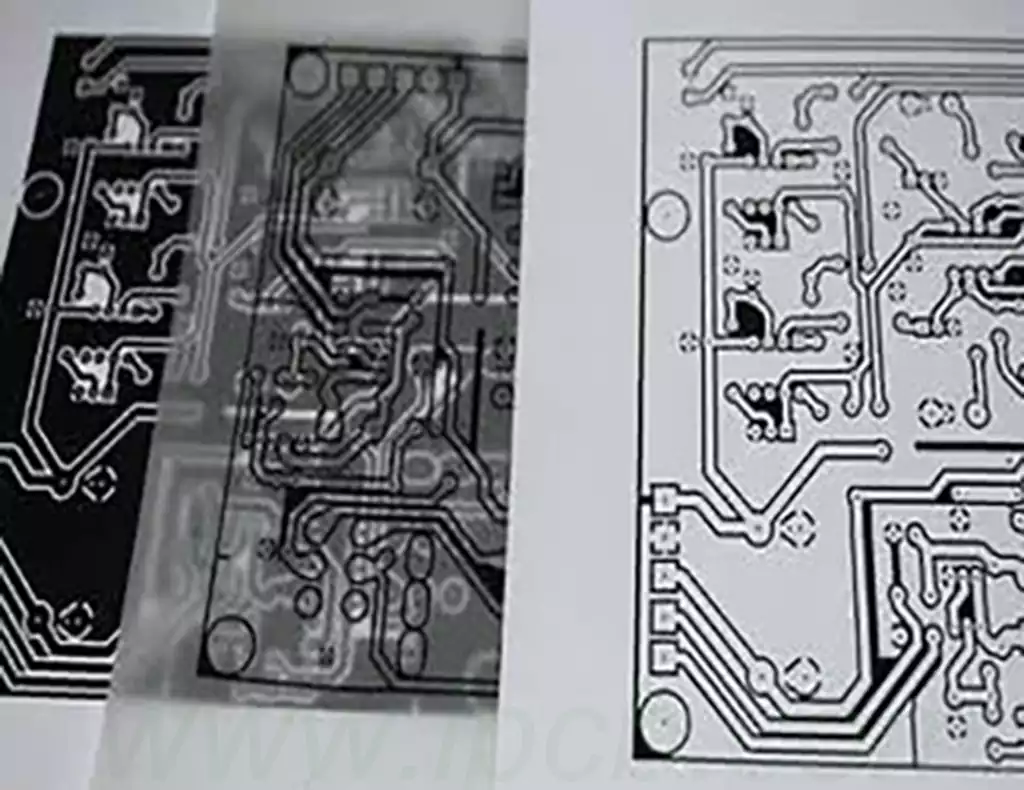
Negative and positive film are two forms of image processes used in the production of printed circuit boards (PCBs). Positive lamination refers to the manufacturing of circuit boards in which drawn lines and patterns are retained and unpainted areas are removed. This process often utilizes alkaline etching, and the end result is that the necessary copper layer is retained on the surface of the board. In contrast, a negative is made by removing the drawn lines and patterns and retaining the copper layer in the undrawn areas. This process usually uses acid etching and results in either clear or black artwork depending on the requirements.
Difference Between negative and positive film:
The negative of a pcb board is often referred to as the Tenting process and the solution used for it is acid etching. In the process of making a negative, the desired wiring or copper surfaces are rendered transparent,while the unwanted portions are shown in black.After exposure in the line process, the transparent areas are chemically hardened by the exposure of the dry film resist to light.Subsequently,the dry film that has not hardened can be washed away by the development process,so that in the subsequent etching process,only the part of the copper foil that has been washed away (i.e., the black portion of the negative) is etched, and the part of the copper foil that has not been washed away by the dry film is retained to form the desired circuit board (the transparent portion of the negative).
In contrast,the positive process for circuit boards is known as the Pattern process and uses an alkaline etching solution.In this case,the desired lines or copper surfaces appear black,while the unwanted areas are transparent.After exposure,the transparent portions are hardened by the light from the dry film,and the unhardened dry film is washed away during the development process.After that,tin-lead is covered on the copper surface exposed after developing in the previous process by a tin-lead plating step,followed by a de-filming operation to remove the hardened dry film.In the subsequent etching process, the alkaline solution removes the copper foil that is not protected by tin-lead (the transparent part of the negative),ultimately leaving us with the circuit board (the black part of the negative).
When distinguishing between the negative and positive film parts of the circuit board,it is first necessary to understand the different types of fiche (negative), including the master, the working, the positive, the negative and the flux side.Generally speaking, the master film is known as black film or silver salt film and is primarily used to duplicate the working film (also known as yellow film or diazo film). Although the working sheet is often in the form of a yellow sheet, it can also be a black sheet, the latter usually being used for high-precision HDI circuit boards or for low volume production to save costs.Yellow sheet, on the other hand, is suitable for general circuit boards and mass production.
When it comes to flux film, the glossy side of black flakes is called flux film, while the opposite is true for yellow flakes.You can distinguish the flux film side by gently scraping the film with a squeegee or razor blade.The negative side of the film with copper on the line is translucent, while the positive side is not. Positive films are commonly used in graphic plating where the lines are removed during development,making the corrosion-resistant layer of the plating primarily lead-tin plated. Negative films, on the other hand, are used for direct etching,where the resist area retained after development forms the line,which is etched directly using an acid etchant.
The effect of the positive film is that all areas where lines are drawn retain the copper layer,while the undrawn areas are removed.The negative,on the other hand,shows that the areas where the lines were drawn are transparent,while the un-drawn portions look black,implying that the copper was retained in these areas.This reversal of effect makes the two different in terms of the scenarios and purposes for which they can be used.
Due to the difference in process and effect,positives are often used in circuits that require high precision such as signal,top and bottom layers .In contrast, negatives are used for large copper layers,especially in power or ground layer designs.
Positive sheets allow for more complex alignment patterns in the design, but may lead to short or open circuit conditions if the design requires moving components or through-hole penetrations . Negatives are better able to avoid such problems because their design is based on a removal approach and is more flexible.
Negative and positive film manufacturing processes play a significant role in circuit board (PCB) performance in terms of line accuracy,signal integrity and production costs.
- Performance Impact of Positives
The positive process is often used for circuit designs with high signal requirements.Due to its ability to preserve the lines that penetrate the transparent portion, the positive wafer process enhances line accuracy,thus ensuring accurate pattern replication.This controlled exposure and development process results in clearer circuit board traces and reduces the risk of shorts and opens. The protective coating in the positive piece in the plating process can also improve the corrosion resistance of the PCB,to ensure that sensitive areas are effectively protected during the etching process. - Chip performance impact
The underlay process is suitable for scenarios where a larger area of copper is required,such as power and ground layers.Negative processes allow copper to be retained in non-linear areas,resulting in wider copper coverage,which improves electrical performance and maintains signal integrity.The direct etch operation of the negative allows the board to excel in the etch process after lead-tin plating, effectively reducing production costs.Although the negative does not perform as well as the positive on high-precision signal layers,it provides an ideal solution for power layers where larger areas are required. - Different Application Scenarios
Positive film is more suitable for high-precision signaling layers because it ensures a clear and accurate line structure and improves the reliability of signal transmission. In contrast, the negative process is more suitable for power or ground layers, where flexible copper coverage strategies improve manufacturing efficiency and cost management. This choice is based on different application requirements and helps optimize PCB performance. - Impact of Production Costs
In terms of production costs, the complex process of positive laminates is generally more expensive, but the high precision signaling provided makes them more valuable for specific applications. Comparatively, the simplified process and expanded copper coverage area of negative laminates allows for more economical production and is an important option, especially in low-volume or general PCB manufacturing.
Considerations for Selecting Negative and Positive film
When selecting negative and positive film in circuit board design, several specific factors need to be considered to ensure the performance and reliability of the final product.
- Circuit Complexity
The complexity of the circuit has a direct impact on the selection of negatives and positive film. Typically, Negatives are better suited for simple circuits and low density designs to ensure design flexibility and checkability. However, for high density circuit layouts or designs that require precise control of line spacing, negatives are more appropriate. - Signal Integrity
Signal integrity is extremely important in high frequency applications. When selecting a negative and positive film, consider the impedance matching of the signal. Positives provide higher resolution and are suitable for circuits that require tight signal integrity, while negatives are better when dealing with large amounts of copper and simple power or ground layers. - Production Costs
Production cost is also a key consideration. Negative processes can often reduce cycle time and material costs. Specifically, negatives tend to be less expensive to produce than positives, can be produced more efficiently by about 3 hours, and can reduce overall costs by as much as 52%. - Design Rules
The accuracy of the circuitry required by the design rules also affects the choice between positive and negative films. Positives usually provide more stringent design rule checks and are therefore suitable for complex signal path designs. Negative film is more suitable for layout optimization and less complex design rule scenarios. - Application Environment and Functional Requirements
The application environment and functional requirements of the final product will directly affect the choice. Positive sheet is often used for circuits with high signal requirements, such as high-speed digital circuits, while negative sheet is generally used for designs with high requirements on copper spreading area, such as power supply and grounding layer {}. Designers need to consider the actual application of the circuit performance requirements to select the appropriate process. - Feasibility and Flexibility
Flexibility and feasibility should not be neglected in the design process. Positives are more flexible and suitable for fast iterative design, while negatives are suitable for stable and accurate mass production design. The designer needs to decide on the structure according to the project schedule and the need for adjustments.
Negative and positive film manufacturing processes each have their own unique importance and application in the manufacturing of printed circuit boards (PCBs). Positives stand out for their high precision and signal fidelity in high-end circuit design,especially for the production of sensitive signal layers. Negatives, on the other hand,show significant advantages in large-area copper and power layer designs due to their extensive copper coverage and lower production costs.