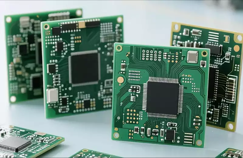
As electronic devices progress towards higher power and miniaturization, PCB thermal management faces severe challenges. Screen printing, once considered merely an auxiliary process for marking and insulation, is now emerging as a crucial support for enhancing PCB heat dissipation efficiency through multi-dimensional innovations in materials, structures, and processes.
Core Objectives of PCB Thermal Management
The primary goal of PCB thermal management is to optimize heat conduction paths and reduce thermal resistance, thereby preventing local overheating that can lead to component failure and shortened lifespans. As a core surface treatment process for PCBs, screen printing influences thermal management effectiveness through three key dimensions:
Thermal Conductivity Variations of the Ink Layer: The inherent thermal conductivity of the ink layer directly alters the surface heat conduction efficiency of the PCB.
Impact of Ink Layer Thickness and Flatness: The thickness and flatness of the ink layer can either hinder or optimize heat diffusion paths.
Application of Functional Screen Printing Inks: These inks can actively enhance heat dissipation capabilities and form tailored thermal management solutions.
Contrary to the traditional perception that screen printing merely serves a marking function, the ink layer it forms is a vital component of the PCB’s heat transfer pathway. Heat from the PCB substrate must pass through the surface medium (including the ink layer) to reach heat dissipation structures such as heat sinks or metal substrates. If the ink layer has high thermal resistance or an uneven structure, it can create a “thermal bottleneck,” causing heat to accumulate beneath components. This issue is particularly pronounced in high-frequency, high-power scenarios like 5G base stations, automotive electronics, and industrial controls, where the heat generation per unit area of PCBs increases by 2-3 times. Consequently, the impact of screen printing on thermal management is significantly amplified, becoming a core variable determining product reliability.
How Screen Printing Influences PCB Thermal Management Efficiency
Ink Material Selection
The material properties of screen printing inks are the primary factor determining their impact on PCB thermal management. Thermal conductivity variations among different ink types can span several orders of magnitude, directly aligning with diverse thermal management requirements.
Conventional solder mask inks (e.g., epoxy resin-based) exhibit relatively low thermal conductivity, typically ranging from 0.1 to 0.3 W/(m·K). These inks are primarily used in low-power PCBs, where their main role is insulation and protection. They offer no active enhancement to thermal management and may even slightly increase surface thermal resistance due to the ink layer coverage. Thus, controlling their thickness is essential to minimize negative impacts.
The advent of functional thermal conductive inks has provided proactive solutions for PCB thermal management. These inks, based on epoxy resin with added thermal conductive fillers like metal oxides (aluminum oxide, zinc oxide), carbon fibers, or graphene, can achieve thermal conductivities ranging from 1 to 10 W/(m·K), with some premium products exceeding 15 W/(m·K). In automotive electronics PCBs, applying thermal conductive inks via screen printing in power device areas can rapidly transfer local heat to substrate edges or heat dissipation structures, reducing hotspot temperatures by 8-15°C. Similarly, in LED driver PCBs, these inks enable uniform heat diffusion, preventing LED chip degradation caused by localized overheating.
Moreover, the high-temperature resistance and thermal stability of inks indirectly affect thermal management outcomes. If inks degrade or crack under prolonged high-temperature conditions (e.g., in automotive engine compartments where temperatures can exceed 125°C), they can disrupt heat conduction paths and even cause insulation failure. Therefore, high-power PCBs require screen printing inks with a high-temperature rating of at least 150°C and no significant degradation after 1,000 hours of thermal aging tests to ensure long-term stability of the thermal management system.
Ink Layer Structure
The thickness, flatness, and coverage of the ink layer formed by screen printing directly regulate heat diffusion paths on the PCB surface, with even minor variations significantly impacting thermal management efficiency.
Ink layer thickness is a critical control point. Conventional marking screen printing typically produces ink layers ranging from 2 to 10 mils (50.8 to 254 micrometers) in thickness. In contrast, thermal conductive ink printing requires precise thickness adjustments based on thermal requirements, usually maintained between 15 and 30 mils (381 to 762 micrometers). Insufficient thickness compromises thermal conductivity, while excessive thickness increases thermal resistance and wastes material.
The impact of ink layer flatness on heat conduction is often overlooked. If the printed ink layer exhibits unevenness, bubbles, or pinholes, it reduces the contact area with heat dissipation structures, increasing contact thermal resistance and decreasing heat transfer efficiency. For instance, bubbles in the ink layer create voids with thermal conductivity close to that of air (0.026 W/(m·K)), acting as localized “thermal insulators” and elevating hotspot temperatures. Optimizing printing parameters and curing processes to ensure an ink layer flatness error of no more than 5 micrometers can effectively reduce contact thermal resistance and enhance heat diffusion efficiency.
Rational design of ink coverage is also essential for optimizing thermal management. In high-power component areas (e.g., MOSFETs, IGBTs), a “local copper exposure + surrounding thermal conductive ink” screen printing scheme can be adopted. The exposed copper areas directly conduct heat, while the thermal conductive ink diffuses edge heat to substrate heat dissipation regions, forming a collaborative heat dissipation structure. In low-power areas, conventional solder mask inks can be retained to balance insulation protection and cost control. This differentiated screen printing design can improve overall PCB thermal distribution uniformity by over 20%.
Process Parameters
Core process parameters in screen printing indirectly regulate PCB thermal management efficiency by influencing the molding quality of the ink layer. Optimizing each parameter enables precise enhancement of thermal performance.
The compatibility between screen mesh count and thermal conductive inks is particularly crucial. Due to the presence of filler particles, thermal conductive inks can cause ink accumulation and uneven particle distribution if the mesh count is too low (<200 mesh). Conversely, excessively high mesh counts (>350 mesh) can filter out some fillers, reducing thermal conductivity. In practice, a 250-300 mesh screen is suitable for most thermal conductive inks, balancing printing precision and filler retention.
The coordinated control of squeegee pressure and printing speed determines the density of the ink layer. Insufficient pressure (<12 N/cm²) results in a loose ink layer with increased internal pores, raising thermal resistance. Excessive pressure (>20 N/cm²) may compress the thermal conductive fillers, disrupting their uniform distribution and reducing local thermal conductivity. Printing speed should match ink viscosity, typically controlled between 50 and 80 mm/s. Excessive speed can introduce air bubbles, while insufficient speed can cause excessive ink penetration into the substrate, affecting insulation performance and heat conduction paths.
Curing processes significantly influence the thermal performance of the ink layer throughout its service life. Thermal conductive inks require curing processes that balance cross-linking degree and filler stability. Thermosetting thermal conductive inks typically undergo baking at 160°C for 80 minutes to ensure a cross-linking degree of at least 92%. Incomplete curing can lead to ink layer aging and cracking, gradually degrading thermal conductivity. UV-curable thermal conductive inks require a UV energy of at least 800 mJ/cm² to prevent localized under-curing and uneven thermal resistance. One industrial control PCB manufacturer improved the thermal conductivity stability of the thermal conductive ink layer by 15% and extended the product’s high-temperature operational lifespan to over 100,000 hours by optimizing the curing profile.
Defect Control
Common defects in screen printing not only affect PCB appearance and insulation performance but can also directly disrupt thermal management systems, leading to localized overheating failures.
Ink pinholes and bubbles are typical thermal management-disrupting defects that can rapidly expand in high-power scenarios, forming “heat accumulation points” and potentially causing adjacent component burnout. To address these issues, source control measures are essential: thoroughly clean the screen and substrate with 0.4 MPa compressed air before printing to prevent impurity incorporation; fully stir the ink and let it stand for 10 minutes to eliminate bubbles; and add a pre-baking step (80°C baking for 20 minutes) before curing to expel volatile substances from the ink layer in advance.
Ink peeling and cracking defects can directly sever heat conduction paths. Under high-temperature conditions, insufficient ink adhesion can cause the ink layer to detach from the substrate surface, exposing substrate areas prone to oxidation and reduced thermal conductivity. Ink layer cracking can fragment continuous heat diffusion paths, creating “thermal islands.” To resolve these issues, optimize surface treatment and ink compatibility: treat the substrate surface with plasma activation to increase surface energy to at least 40 dynes/cm; select dedicated thermal conductive inks compatible with the substrate material (e.g., FR-4, aluminum substrates) and ensure no ink peeling in adhesion tests (3M 610 tape peel test).
Position shift defects significantly impact high-precision PCBs. If thermal conductive ink printing shifts and fails to fully cover high-power component areas, heat cannot be effectively conducted, causing sudden hotspot temperature increases. If ink intrudes into heat dissipation holes or pad areas, it can block heat diffusion channels and affect connections with external heat dissipation structures. During production, employ a visual positioning system to assist printing, ensuring ink coverage position deviations of no more than 0.1 mm. Additionally, strictly adhere to the IPC-2221 standard and reserve sufficient clearance for heat dissipation holes and pads.
Emerging Trends in Screen Printing for PCB Thermal Management
As PCB power density continues to rise, screen printing technology is evolving towards “precision, functionality, and intelligence,” offering more efficient thermal management solutions.
The application of digital screen printing technology enables personalized zonal printing of thermal conductive inks, precisely controlling ink thickness and coverage based on the thermal requirements of different PCB areas. This approach overcomes the limitations of traditional stencil processes and is particularly suitable for low-volume, customized high-power PCB production, enhancing thermal management solution flexibility by over 30%.
The development of novel functional inks further expands the thermal management potential of screen printing. Graphene-modified thermal conductive inks, with ultra-high thermal conductivity (≥20 W/(m·K)), have become the preferred choice for high-end automotive electronics and aerospace PCBs. These inks can form ultra-thin thermal conductive layers (thickness ≤100 micrometers) via screen printing, improving thermal performance without affecting overall PCB thickness. Phase-change thermal conductive inks can form “adaptive heat dissipation layers” through screen printing, absorbing heat through phase changes when temperatures rise and reducing hotspot temperatures, making them suitable for intermittent high-power scenarios.
The widespread adoption of intelligent process control systems enables real-time optimization of screen printing thermal performance. Online thermal resistance monitoring devices can detect thermal resistance data of the cured ink layer in real-time and automatically adjust parameters such as squeegee pressure and curing temperature. Machine vision inspection systems combined with AI algorithms can accurately identify minute pinholes, bubbles, and other defects with an accuracy rate exceeding 99.5%, preventing defective products from entering downstream processes. The integration of these technologies shifts screen printing process control for PCB thermal management from “passive correction” to “active optimization.”
In the iterative process of PCBs towards higher density, higher power, and miniaturization, thermal management has emerged as a core bottleneck restricting product performance. As a key process throughout PCB production, screen printing is evolving from an “auxiliary process” into a “core thermal management empowerment link.”