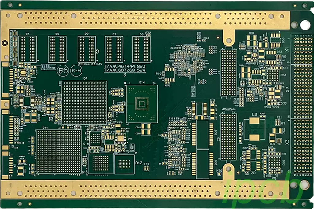
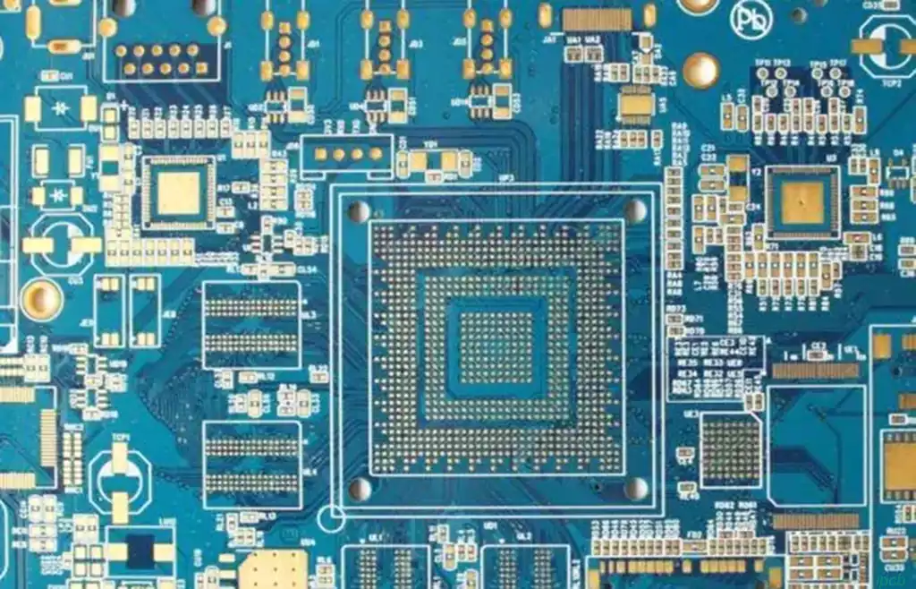
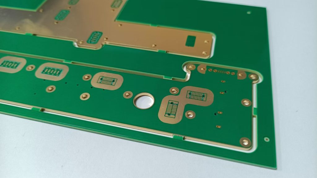
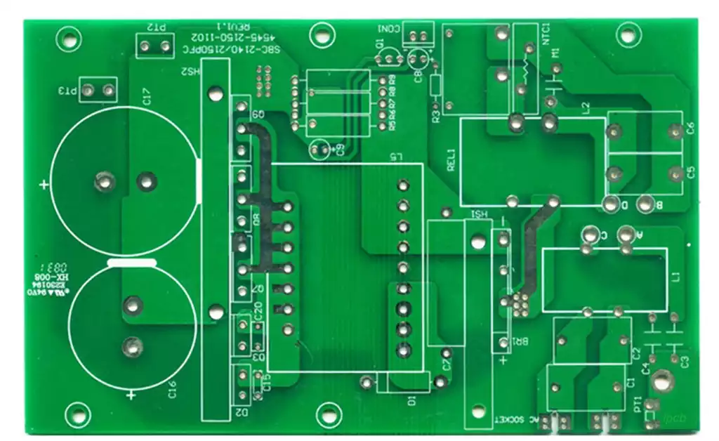
A packaging substrate is a thin sheet, usually made of insulating material, used to hold and connect electronic components. It carries the electrical connections between electronic components and ensures that these components operate stably and efficiently when in operation. It can be simply understood as a PCB or thin thick-film circuit substrate with higher performance or special features. This substrate plays a chip and conventional printed circuit boards (mostly motherboards, vice boards, backplane, etc.) between the different lines of the electrical interconnections and transitions, but also for the chip to provide protection, support, heat dissipation, assembly and other effects.
The role of the packaging substrate:
Carry IC chips;
Protecting, fixing and supporting the IC chip and providing heat dissipation channels;
There are lines inside, which is the bridge between the chip and PCB;
Can be buried in passive, active devices to achieve certain system functions.
Packaging pcb for the current mainstream production process for the improved semi-additive method. First of all in the substrate with ultra-thin base copper laminated to the dry film using a positive piece of graphic transfer, and then through the formation of graphic plating additive line, and finally remove the dry film and the base copper to complete the high-precision wiring. The key control points of the technology are bottom copper uniformity, graphic resolution, plating uniformity, film removal and copper fading.
Chip packaging process can be divided into the following steps:
Chip cutting
First in the chip on the back of the blue film and placed on top of the iron ring, and then sent to the chip cutter for cutting, the purpose is to use the cutter to cut the chip on the wafer separated into individual grains.
Die sticking
First of all, the grains will be glued to the wire frame, also known as grain holder, preset to extend the IC grain circuit extension foot, with silver glue on the grains for adhesive fixation.
Soldering
The contact point on the grain is the first soldering point, and the contact point on the internal pin is the second soldering point, first burn the end point of the gold wire into a small ball, and then press the ball to weld on the first soldering point. Next, according to the designed path to pull the gold wire, the gold wire pressure welding on the second point to complete a gold wire welding action. The purpose of the welding line is to connect the contacts on the grain with gold wire or aluminum wire copper wire to the pins within the wire frame, so that the circuit signal of the ic grain is transmitted to the outside world.
Sealing
The wire frame preheating, and then the frame on the die-casting machine on the encapsulation mold, and then half dissolved resin squeezed into the mold, resin hardening will be able to open the mold to take out the finished product. The purpose of sealing is to prevent moisture and other intrusion from the outside, effectively discharging the heat generated inside the outside, to provide a shape that can be held.
Cutting and molding
After sealing, you need to remove the excess residual glue on the wire frame, after plating to increase the conductivity of the outer pins and oxidation resistance, and then cut the foot molding. The wire frame has been encapsulated on the die, shear separation and unwanted connection materials removed.
After cutting the foot molding, a chip packaging process is basically complete, the follow-up also requires some processing in order to make the chip can work stably and efficiently, including de-gumming, de-wefting, de-framing, etc., and then finally test and inspection, after all the processes are completed, to ensure that there is no problem with the chip, the chip will be able to work normally at this time.
Packaging substrate as one of the core components of electronic equipment, for the performance and reliability of electronic products play a vital role.