In the PCB industry, 1OZ copper thickness means the thickness of 1OZ of copper uniformly laid flat over an area of 1 square foot (FT2). It is the average thickness of copper foil expressed in terms of weight per unit area. It is expressed by the formula, i.e.,1OZ = 28.35g/ FT2 (FT2 is square feet, 1 square foot = 0.09290304 square meters).
Specifically, it and the length can also be said that the thickness of the conversion method is as follows:
First, we know the density constant of copper and the related unit conversion formula is as follows:
The density of copper ρ = 8.9g/cm3
1 centimeter (cm) = 10 millimeters (mm); 1 millimeter (mm) = 1000 microns (um)
1mil≈25.4um
1 FT2≈929.0304 cm2
1mil≈25.4um
According to the formula of mass m = ρ × V (volume) = ρ × S (area) × t (thickness), we know that the weight of the copper foil divided by the density of copper and the area of the copper foil thickness!
From the previous section, we also know that 1oz = t × 929.0304cm2 × 8.9g/ cm3 = 28.35g/ cm2
So, t = 28.35 ÷ 929.0304 ÷ 8.9cm ≈ 0.0034287cm = 34.287um ≈ 34.287 ÷ 25.4mil ≈ 1.35mil
This shows that the thickness of 1oz copper foil is about 35um or 1.35mil.
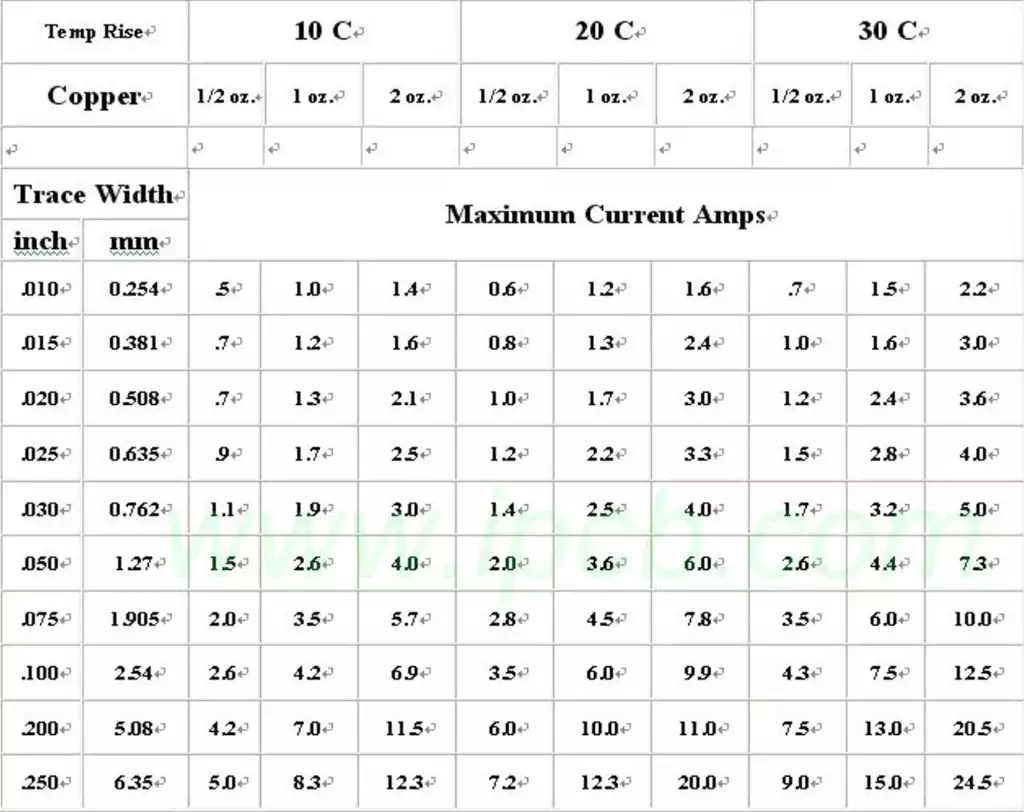
In PCB design, the relationship between the thickness of the copper foil of the board,the width of the alignment and the amount of current that can be passed is closely related:
Copper Foil Thickness: Copper foil thickness refers to the physical thickness of the copper foil,usually expressed in ounces (oz).1 ounce is equal to 0.00144 inches, so, for example, 1 ounce of copper foil is approximately 0.018mm thick. copper foil thickness directly affects the mechanical strength, thermal conductivity and electrical properties of the circuit board.Thicker copper foils can withstand higher currents,but they also increase the weight and cost of the printing circuit board. Usually, thicker copper foils are chosen to withstand higher currents, taking into account the electrical properties and mechanical strength to meet the requirements.
Alignment Width:The alignment width refers to the width of the wires on the PCB board. The width of the alignment is the same as the thickness of the copper foil,which also affects the electrical performance and mechanical strength of the PCB. Wider alignments can withstand higher currents,but too wide an alignment may affect the PCB’s wiring density and signal quality.Generally speaking, the width of the alignment should be reduced as much as possible under the premise of meeting the electrical performance requirements in order to reduce the area and cost of the PCB substrate.
Passable Current Size: The passable current size of a copper foil depends on its thickness and cross-sectional area.If the thickness of the copper foil and the width of the alignment are determined,the amount of current that can be passed depends mainly on the cross-sectional area of the alignment. According to Ohm’s law, the amount of current is inversely proportional to the resistance,which in turn is related to the length,resistivity and cross-sectional area of the wire. Therefore, in order to pass a larger current,a thicker alignment or thicker copper foil is required.
Overall, in PCB design, the relationship between the 1OZ copper thickness of the copper foil of the circuit board,the width of the alignment, and the amount of current that can be passed is mutually restrictive. Reasonable design choices need to be made according to actual needs and constraints.