The pcb aspect ratio, which is the ratio of the length to the width of the circuit board, is a critical parameter in electronic design. The aspect ratio refers to the ratio of the length to the width of the circuit board, and it not only affects the physical dimensions and layout of the circuit board but also directly impacts its performance and application effectiveness.
The PCB aspect ratio has a significant impact on circuit board performance. On one hand, an appropriate aspect ratio helps optimise the thermal design of the circuit board, improve heat dissipation efficiency, thereby reducing the operating temperature of the circuit board and extending its service life. On the other hand, the choice of aspect ratio also affects the mechanical strength and stability of the circuit board. An excessively large aspect ratio may cause the circuit board to bend or deform when subjected to external forces, thereby affecting the normal operation of components on the circuit board.
The aspect ratio plays a crucial role in the electroplating process during PCB manufacturing. The electroplating solution must flow effectively within the drill holes to achieve the desired copper plating. Holes that are significantly smaller than the board thickness can result in uneven or unsatisfactory copper plating. The larger the aspect ratio, the more challenging it becomes to achieve reliable copper plating within through-holes. Therefore, a smaller aspect ratio leads to higher PCB reliability. At Sierra Circuits, we offer a 0.75:1 aspect ratio for microvias.
The pcb aspect ratio is the ratio of the board thickness to the diameter of the through-hole. This is an important ratio because it affects plating within the through-hole (also influenced by the ring).
Assuming your PCB thickness is 0.2 inches and the through-hole diameter is 0.02 inches. The aspect ratio would be 10:1. As this ratio increases, more plating surrounds the through-hole compared to the internal drilled portion, thereby increasing the risk of cracks forming during soldering due to z-axis expansion. Maintaining a lower PCB aspect ratio ensures uniform plating throughout the through-hole and provides higher strength throughout the PCB’s entire service life.
Most PCB manufacturing facilities can achieve an aspect ratio of 6:1. The minimum practical drill hole diameter is approximately 0.013‘ floating, resulting in a maximum board thickness of approximately 0.078’.
When considering reducing the aspect ratio, both board thickness and minimum drill hole diameter should be considered simultaneously, which may save you from a lengthy and confusing manufacturing issue. Additionally, your vias will be more robust and provide more connection space for component installation.
Design Considerations for PCB aspect ratio
Aspect ratio is one of the key factors affecting signal transmission performance.
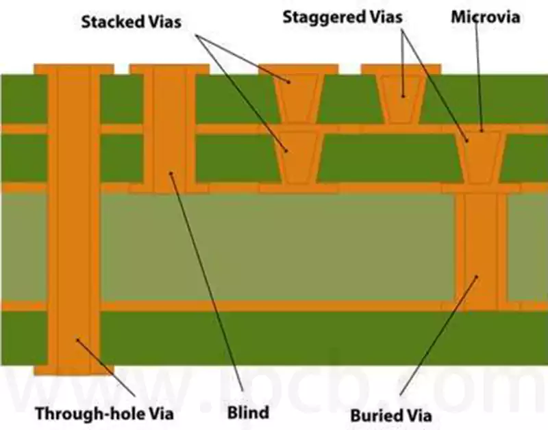
High-speed signal transmission: For high-speed signal boards, a smaller aspect ratio helps reduce signal loss. When signals are transmitted through vias to another layer, the vias create excess copper stubs, which can cause signal reflection, scattering, and delay, thereby affecting signal integrity. The longer the stub, the greater the impact on signal transmission. Blind vias and buried vias can help manage the PCB aspect ratio by reducing the number of layers and limiting trace changes, thereby providing clearer signal transmission paths and reducing parasitic capacitance.
Impedance control: High aspect ratio conductive paths help reduce resistance, improve current flow efficiency, and achieve specific impedance values, which are critical for signal matching and reducing reflections. By placing signal traces and ground planes close to each other, the impedance of different traces can be controlled.
The choice of aspect ratio is also closely related to manufacturing costs and manufacturability.
Drilling Costs: Drilling costs are directly related to the thickness of thick copper. Excessively high aspect ratios can increase plating and drilling issues during the manufacturing process. For example, as via diameter decreases and thickness-to-diameter ratio increases, ensuring uniform metal coverage inside the hole becomes more challenging.
Via type: Using blind vias and buried vias can help designers meet the high-density constraints of traces and pads in high-density interconnect (HDI) PCBs without increasing the total number of layers or PCB size. However, compared to PCBs using standard through-holes, blind vias and buried vias have higher manufacturing costs because they increase PCB complexity and manufacturing steps, requiring more frequent testing and precision checks.
Number of Layers: The more layers a PCB board has, the higher the manufacturing cost. Typically, an 8-layer board costs 50%-70% more than a 6-layer board. Increasing the number of layers adds complexity to design and manufacturing, so a trade-off between performance and cost must be considered.
Supplier Capability: PCB suppliers typically require that the aspect ratio of their drill holes does not exceed 10:1. If the PCB’s aspect ratio exceeds 10, it is necessary to consider whether the supplier has the production capability.
Dimensions, spacing, aspect ratio, the number of holes on the board, and machine type (e.g., laser drilling) are all factors to consider in PCB design.
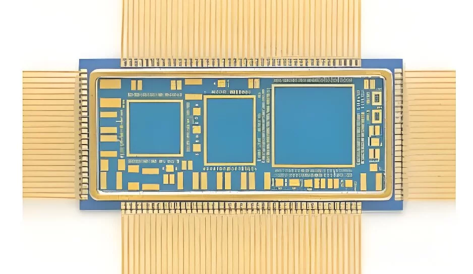
Microvias: In HDI PCBs, microvias are a key technology, and the aspect ratio refers to the relationship between the dielectric isolating the copper layers and the hole diameter. Most suppliers require an aspect ratio between 0.6:1 and 1:1, with 0.8:1 being the most common. Ultra-thin PCB materials can achieve smaller vias, less copper plating, smaller spaces and traces, and lower via aspect ratios.
Hole size: The minimum drill width for standard vias is 20 mils, with a ring width of 7 mils and an aspect ratio of 6:1. However, this may be difficult to achieve for many circuit boards.
The aspect ratio is also related to the mechanical strength and long-term reliability of the PCB boards.
Plating quality: The aspect ratio is critical for plating inside vias, as it affects plating uniformity. Copper-free holes are a functional issue for PCBs, and the high precision required for the aspect ratio creates a cost-quality trade-off for PCB manufacturers and poses serious quality risks for downstream customers. Ensuring the uniformity of metal in the holes and protecting the metal from damage during subsequent processing is important.
Vibration factors: Among the factors causing electronic device failures due to mechanical forces, electromagnetic forces, and environmental conditions, 27% are caused by vibration factors. Long-term vibration environments can shorten the operational lifespan of PCB boards. Therefore, in PCB design, considerations must extend beyond trace density and trace accuracy to include the dynamic performance of the circuit board.
The PCB aspect ratio is one of the core elements in circuit board design, significantly influencing signal integrity, manufacturing costs, mechanical strength, and long-term reliability. Carefully selecting and controlling the aspect ratio is the foundation for achieving high-performance, high-reliability electronic product design.
Designers must balance multiple dimensions, including signal transmission, manufacturing costs, and mechanical strength, to determine the most suitable aspect ratio. This comprehensive consideration can effectively enhance the overall performance and reliability of the circuit board, ensuring its stable operation in various application scenarios.
Therefore, a deep understanding and reasonable application of PCB aspect ratio design principles are crucial for the successful development of high-quality electronic products that meet stringent requirements.