How to power supply
When we design pcb board products, after understanding the demand, the first thing to design is the product power supply system, whether it is a product, or chip IC, pcb board power supply this step is essential.
When designing the pcb board board power supply system, the first step to consider is the size of the power supply voltage and current needed for each module, that is to say, how much power is needed. Circuit board power supply usually use two kinds of electricity, respectively, strong and weak electricity. Here the weak power is lower than the human body’s safety voltage of 36V voltage of electricity, strong power is high with 36V electricity, if in the usual way we say that the strong power usually refers to 220V alternating current.
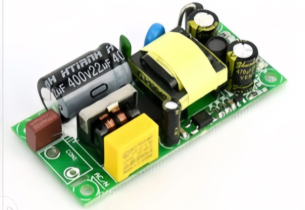
For strong electricity we can get directly from the utility 220V. For weak power, we can buy the corresponding power adapter module on the market, of course, you can also directly design the adapter.
What determines the power integrity in a pcb board?
Power integrity is a concept in both AC and DC; in the case of DC, we are concerned about the proper sizing of the copper wires to ensure low DC voltage drop. If a PCB board is designed without considering power integrity, the voltages observed on the power rails may be as shown below. During the phase of I/O switching, current pulses pulled from the PCB board’s power supply network (PDN) can excite transients on the power bus.
Today, it is very difficult to design a high-speed electronic system successfully without a thorough knowledge of the chip, package structure, and PCB board power supply system characteristics. In fact, in order to meet lower supply voltages, faster signal flip-flops, higher levels of integration and many more challenging requirements, many companies at the forefront of electronic design have invested a great deal of money, manpower and material resources into the analysis of power supply systems in order to ensure the integrity of the power supply and signals during the product design process.
Power supply system (PDS) analysis and design is becoming increasingly important in the field of high-speed circuit design, especially in the computer, semiconductor, communications, networking and consumer electronics industries. With the inevitable further isotropic shrinkage of ultra-large scale integrated circuit technology, the supply voltage of integrated circuits will continue to decrease. As more and more manufacturers move from 130nm technology to 90nm technology, it is foreseen that the supply voltage will drop to 1.2V or even lower, while at the same time the current will increase significantly. From DC IR voltage drop to AC dynamic voltage fluctuation control, this development trend poses a great challenge to the design of power supply systems as the allowable noise range becomes smaller and smaller.
Typically in AC analysis, the input impedance between the pcb board power supply and ground is an important observation used to measure the characteristics of the power supply system. Determination of this observation evolves into the calculation of the IR voltage drop in DC analysis.
In both DC and AC analyses, the factors that affect the characteristics of the power supply system include the layering of the PCB, the shape of the power supply board layer planes, the layout of the components, the distribution of vias and pins, etc. The concept of input impedance between power supply grounds is an important observation for measuring the characteristics of the power supply system.
The concept of input impedance between power supply and ground can be applied in the simulation and analysis of the above factors. For example, a very broad application of power ground input impedance is to evaluate the placement of decoupling capacitors on a board. With a certain number of decoupling capacitors placed on the board, resonances specific to the board itself can be suppressed to reduce noise generation, and board edge radiation can be reduced to mitigate EMC problems. In order to improve the reliability of the power supply system and to downgrade the manufacturing cost of the system, system design engineers must always consider how to cost-effectively select the system layout of decoupling capacitors.
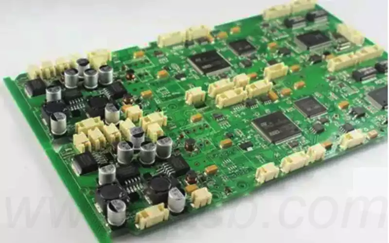
The pcb board power supply system in a high-speed circuit system can usually be divided into three physical subsystems: the chip, the integrated circuit package structure and the pcb board. The power grid on the chip consists of several metal layers placed alternately, each layer of metal by the X or Y direction of the metal strip to form the power or ground grid, the vias will be different layers of metal strip connection.
For some high-performance chips, no matter the core or IO power supply are integrated with a lot of decoupling unit. The IC package structure, like a scaled down pcb board, has several layers of complexly shaped power or ground plates. On the upper surface of the package structure, there is usually a place for decoupling capacitors to be mounted. pcb boards usually contain a continuous area of large power and ground plates, as well as a number of discrete decoupling capacitor components of various sizes, and power supply rectifier modules (VRMs). Bonding wires, C4 bumps, and solder balls connect the chip, package, and pcb board together.
Good thermal design is critical to the reliable operation of pcb board power supply products.
When laying out the pcb board, it is necessary to keep the power devices that generate large amounts of heat away from temperature-sensitive components, and at the same time, keep good heat dissipation paths around the heat source components.
For small power circuits, you can increase the area of the external heat sink and increase the area of copper foil layer inside the PCB board to improve the natural convection heat dissipation.
For high-power circuits, it is necessary to use fan forced air convection cooling, and combined with a suitable heat sink for thermal design.
Reasonable pcb board layout is also very important for the realization of high-performance power supply design.
Wiring needs to pay attention to high-frequency, high-energy current path loop area control at a minimum, in order to reduce high-frequency electromagnetic radiation. At the same time, magnetic components, power switches and other devices away from analog control circuits, to avoid magnetic and electric fields on its interference. For high-frequency switching joints, you can use solder-resistant holes or gaps in the way of wiring to reduce cross-coupling. For coupled inductors and other magnetic devices, you can set up a magnetic shield or isolation layer. The entire power supply circuit to use a separate ground plane to reduce ground impedance.
To reduce the impedance of the pcb board power supply system, some of the following design guidelines should be followed:
- decrease the spacing between the power supply and the floor layer;
- increasing the size of the flat plate;
- increase the dielectric constant of the filler medium;
- using multiple pairs of power supplies and floor layers.
However, due to manufacturing or other design considerations, design engineers need more flexible and effective ways to change the impedance of the power supply system. To reduce impedance and eliminate those resonant peaks, discrete decoupling capacitors placed on the PCB become a common method.
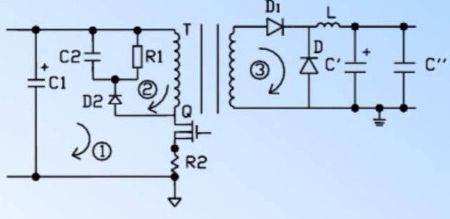
PCB board Power Supply Design
The design of a pcb board power supply is more than just converting AC power to DC power. The function of a power supply is to provide power to circuit components at the correct voltage and current. Voltages as low as 1.8 and 1.2V devices will still be more common in the future. After all, low voltages are less tolerant of power supply noise. Power supplies also need current limiting to limit the maximum current. Therefore the important parameters of a power supply are voltage, maximum current, voltage ripple and heat loss at maximum current.
Here are 7 things to consider when designing power supplies for pcb boards:
1.the right voltage regulator
Generally, a linear regulator or switch mode regulator is selected. Linear regulators improve low noise output, but dissipate more heat and require a cooling system. Switching mode regulators are efficient over a wide current range, but switching noise can cause spikes in the response.
2.pcb board power supply thermal management
The performance of the power supply depends directly on the heat dissipation, most electronic components will heat up when current is passed through them. The amount of heat emitted depends on the power level, characteristics and impedance of the component. A suitable voltage regulator can reduce heat dissipation in the circuit. Switching regulators are very efficient because less heat is emitted.
If a linear regulator is chosen, a heat sink or other cooling method is recommended, and if the device is dissipating a lot of heat, a fan may be considered. Heat dissipation may not be uniform across the pcb board, and components with high power ratings may emit a lot of heat, creating hot spots around them. Heat sinks can be used near the components.
3.Ground and power layers for better pcb board power supply
Ground and power layers are low impedance paths used for power transmission. Power supplies require a separate grounding layer to distribute power, reduce EMI, minimize crosstalk and reduce voltage drop. The power supply layer is dedicated to transferring power to the desired area of the pcb board.
Each part of the grounding network needs to be handled separately. In multilayer pcb boards, one or more layers can be dedicated to the ground and power layers. In addition, interference and crosstalk can be reduced by placing a step ground layer between 2 active signals, thus effectively surrounding the signal alignment with ground.
Decoupling primarily reduces the impedance between the power supply and ground, with the decoupling capacitor acting as an auxiliary power supply to provide the current required by the IC. The decoupling capacitor acts as a local charge source and supports switching. All decoupling capacitors must be connected close to the IC’s power supply pins, with the other end connected directly to a low-impedance ground layer. It is necessary to connect the decoupling capacitor and the grounding hole using a short walkway to minimize the series additional inductance of this connection.
4.decoupling capacitors and bypass capacitors
When power is distributed to components across the board, different active components will cause ground bounce and ringing in the power rails. In this case, care should be taken to use decoupling and bypass capacitors near the power supply pins to meet the short spikes in equipment current demand.
5.EMI filtering
Everyone wants the EMI level of the power supply to stay below their defined spectral limits. Therefore, use EMI filters at the power input point to reduce conducted noise.
6.Frequency Response of Power Transmission System
When a power supply is suddenly loaded, for example from no load to full load, the voltage output will tend to drop briefly and return to normal voltage. In some cases, the output will oscillate for a period of time before the voltage stabilizes to normal. If the oscillations are out of design limits, the output capacitors and compensation capacitors will need to be adjusted. For better circuit design response, make sure the selected components are within the design limits. Circuits respond differently whether they are AC or DC. AC and DC circuits should be considered separately.
7.Power Integrity (PI)
Power Integrity is the quality of power delivered to a circuit. It measures the efficiency with which power is transferred from the power supply to the loads within a system, ensuring that all circuits and devices are supplied with the proper amount of power to achieve the desired performance of the circuit. A less noisy power supply ensures higher power integrity. Power integrity design is nothing more than managing power supply noise.
Generalization
pcb board power supply can be the source of most thermal and noise problems in pcb boards, so board design must take this into account from the start. Great board design starts with a good pcb board power supply layout.