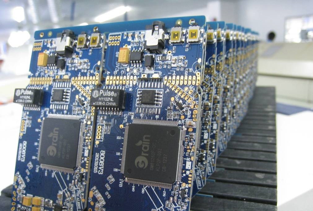
pcb board scrap refers to the waste materials generated during the manufacturing or disposal of printed circuit boards (pcb).
These wastes usually include the following types:
Scrap generated during the production process: including pcb board edges, test boards, defective boards and so on. These wastes may be discarded because of defects in the production process or because they do not meet specifications.
Scrap from recycling process: when old pcb boards are recycled and disposed of, some scrap will be generated, such as soldering residue, insulation layer, copper foil, etc.
Electronic component waste: pcb boards on the electronic components in the disassembly or replacement of the waste generated, such as no longer used components, welding residues, etc..
Chemical waste: pcb production process used in the chemicals (such as etching solution, cleaning agent) in the treatment and cleaning process of the waste generated.
pcb in the production and use of the process of waste generated by the reasons involved in a number of aspects. The following are the main reasons and their associated waste types:
- Scrap during production
Cutting and Punching: During the production of pcb, raw materials such as copper foil and insulation boards are cut and punched. The edges and scrap from these cutting and punching processes are discarded.
Etching: In the etching process, chemicals are used to remove unwanted layers of copper to form circuit patterns. These chemicals and the waste solution generated during the etching process, as well as copper residues, are scrap.
Soldering: The soldering process produces solder residues and solder defective boards, which can become scrap.
Test and Inspection: Defective pcb boards or test boards that do not meet specifications found during the test and inspection process are also discarded. - Scrap in use and maintenance
Failure of electronic components: In the course of use, if the electronic components on the pcb fail or are damaged, they may need to be replaced, which will generate scrap electronic components and pcb boards.
Equipment upgrading: when equipment is upgraded or replaced, old pcb boards and electronic components may be replaced, generating scrap. - Waste in the recycling process
Dismantling: When recycling old pcb boards, the boards are dismantled by physical or chemical methods to separate out copper, plastic, glass fibers and so on. The fragments and residues generated by this process are also waste materials.
Handling residues: In the recycling process, residues generated from the handling process, such as chemical wastes and impurities after handling, also become waste. - Environmental and regulatory requirements
Heavy metals and hazardous substances: pcb boards may contain hazardous substances such as lead, cadmium, mercury, etc. These substances require special treatment to avoid harming the environment and human health. The process of handling these hazardous substances may generate specific waste materials. - Production efficiency and loss
Production loss: in the pcb production process, due to design defects, process problems or operational errors resulting in nonconforming products or loss will also be converted into scrap.
The composition and bonding of pcb’s and their impact on their recycling
What is in a pcb? There are solder resist inks and silkscreen on the outer layer, copper foil on the inner layer, different surface treatments, different types of epoxy resins, and so on. All of these components are integrated together, and frankly, separating them is a big challenge. Currently, the only way to do this is to grind the entire pcb bare board into a granular mixture of metal, fiberglass, and resin. Today, we are able to separate metals, such as copper and gold, from this, purify them and reuse them.
But most of the remaining residue, a mixture of resin and fiberglass particles, ends up in landfills. In some countries, these residues can also be used for energy production. Of course, the ideal scenario would be to reuse these residues in the manufacture of new products, and research is currently underway in the industry with the ultimate goal of separating the glass fibers from the mixed particles and reusing them as raw materials for pcb substrates.
Separating resin and glass fiber, a well-known board manufacturer in China has developed a FR4-type glass fiber substrate suitable for separating glass fiber and resin, but as of now, this material is still in the laboratory stage. Again, when we talk about recycling of pcb, we should be referring to the possibility of separating the glass fibers and resins from the organic residues and to what extent they can be reused in pcb production. pcb board scrap has many potential uses and ways of reuse after processing and recycling. These wastes can be converted into a variety of useful resources and some of the main uses are listed below:
- Metal recycling
Electronic scrap is pre-treated to remove components such as silicon wafers, poles, resistors, etc., crushed, and sent to incinerators to be burned with air or oxygen to remove organic matter. Then transferred to the copper smelting furnace with the crude copper material together with the melting, so that the precious metals and non-ferrous metals to generate copper alloys, ceramic materials in the waste and glass fibers, etc. were slag discharged. Will be enriched with precious metals of copper alloy melt cast into anode, by electrolysis, from the anode mud recovery of gold, silver, palladium, its recovery rate are greater than 90%.
The pcb boards contain a variety of precious metals such as copper, gold, silver and palladium. These metals can be extracted through specialized recovery techniques (e.g. pyrometallurgy, hydrometallurgy, etc.) and reused to manufacture new products.
Copper: Copper recovered from pcb boards can be used in the manufacture of wires, cables, electronic components, etc.
Precious metals: recovered gold and silver can be used in jewelry, electronics and other high value applications. - reprocessed materials
Crushing and granulation: Crushed pcb scrap can be used as fillers or additives for other industrial materials. For example, pulverized pcb scrap can be used as a reinforcing material for concrete or as a filler in plastic composites.
Composites: The processed pcb board scrap (e.g. fiberglass) is used to make composite materials, which can be used in automotive, construction and other fields. - electronics
Remanufactured components: some still intact electronic components and assemblies can be disassembled from waste pcb boards, tested and repaired and reused. - environment and soil improvement
Soil amelioration: properly treated pcb waste (especially those parts that contain organic materials) can be used for soil amelioration or as a soil conditioner, but this needs to be done to ensure there are no hazardous substances left to avoid negative impacts on the environment. - Art and decoration
Creative arts: pcb scrap can be used by artists and artisans to produce creative artworks, decorations or crafts that showcase the aesthetics of technical and electronic scrap. - energy recovery
Incineration: In some cases, treated pcb scrap can be incinerated to generate electricity, but this method needs to be carefully controlled to prevent the release of harmful gases and ash. - New Product Development
Green chemicals: useful chemicals extracted from pcb board scrap can be used to develop new environmentally friendly chemicals or materials.
Important Notes
Safety and environmental protection: When handling pcb scrap, environmental regulations and safety norms must be strictly followed to ensure that hazardous substances (e.g., lead, cadmium, mercury, etc.) are handled and disposed of in a safe manner to avoid harm to the environment and human health.
Certifications and regulations: Companies that handle and reuse pcb waste should follow relevant environmental certifications and regulations to ensure the legality and environmental friendliness of their operations.
At present, the recycling and treatment methods for waste pcb and pcbA mainly include physical, chemical and biological methods. Physical method mainly includes mechanical crushing, air sorting and magnetic adsorption and other technologies; chemical method is divided into pyrometallurgy, hydrometallurgy and so on.
1.pcb paint removal.
pcb surface is generally coated with a layer of paint to protect the metal, recycling treatment should be removed before the paint. Paint strippers have organic paint strippers and alkaline paint strippers, organic paint strippers are highly toxic and harmful to human body and environment, alkaline paint strippers are relatively less toxic. We get the best formula for paint removal through experiments: put the cut pcb piece into 10% sodium hydroxide solution. Add 0.5% additives A, 0.5% additives B, 0.05% of the corrosion inhibitor mercaptobenzotriazole, water bath heating, the surface of the paint can be completely removed within 30min, can be further recycled on the bare metal. Alkaline paint stripping is the paint and circuit board contact with the place to separate the paint is still mainly to the original structure exists, can be recycled.
2.pcba recycling treatment of physical method
Physical method is based on the material density, conductivity, magnetism, surface wettability and other physical characteristics of the differences in recycling. The main processes are dismantling, crushing, sorting, recovery of precious metals, treatment of hazardous substances.
The general order of selective dismantling of dismantled e-waste is as follows: Selection of reusable parts. Dismantle the hazardous components and categorize the parts of various materials. The dismantling methods are manual dismantling, mechanical dismantling, automatic dismantling. pcb’s automatic dismantling adopts methods such as bath washing or hot air heating to dissolve solder, and then use vacuum clamps or robots to remove pcb’s surface components.
Crushing. pcb crushing has impact crushing, extrusion crushing and shear crushing. Currently the more successful application of ultra-low temperature freezing and crushing technology, can be tough materials at low temperatures after the brittle crushed to 0.074mm, so that the metal and non-metal completely dissociated. Domestic often use two-stage crushing technology, that is, with a shear crusher coarse crushing, and then dry or wet crusher pcb particles finely crushed to the required size, to achieve complete dissociation of metal and non-metal.
Sorting will be crushed substances according to the density of each component, particle size, magnetic conductivity, electrical conductivity and other characteristics of the differences in sorting, usually dry and wet sorting. Dry sorting includes dry screening, magnetic separation, electrostatic, density and eddy current sorting. Wet sorting has hydraulic cyclone classification, flotation, hydraulic shaker and so on. Wet sorting recovery rate is high, but the cost is also high, the reagents used to pollute the environment, after sorting the waste residue waste liquid on the environment caused by secondary pollution. Dry sorting is relatively low-cost, low pollution, the main drawback is that the sorting rate of fine particles is low.
Density sorting: the movement of particles in the fluid depends not only on the particle density, but also on its size and shape. To minimize the scale effect and control the relative movement of particle density. The metal in pcb is separated and enriched, and the effect of airflow sorting and enrichment of metal under different particle sizes is examined.
Disposal and recycling of pcb board scrap is critical for environmental protection, as these wastes may contain hazardous substances such as lead, cadmium, mercury and other heavy metals. Effective recycling and treatment methods include:
Mechanical separation: physically separating different materials on pcb boards such as copper, plastic and fiberglass.
Chemical treatment: using chemical reactions to break down or dissolve hazardous substances in pcb boards.
Thermal treatment: Breaks down pcb boards and the hazardous substances attached to them through high temperature incineration or heat treatment.
Many countries and regions have environmental regulations and recycling standards aimed at reducing the environmental impact of pcb waste.
By effectively recycling and reusing pcb board scrap, not only can we reduce the waste of resources, but also reduce the impact on the environment.