Generally speaking, when designing ordinary single-sided and double-sided boards, there is no need to consider the pcb board stack up problem. Usually, copper clad boards with copper thickness and board thickness that meet the design requirements are directly selected for direct processing. However, when designing PCBs with more than 4 layers, the stacking design directly affects the performance and price of the PCB.
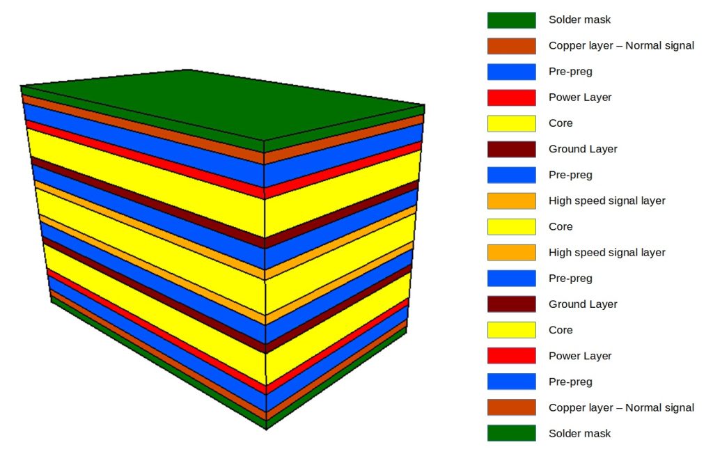
Multilayer PCBs are made of copper clad core boards (Core), prepreg (PP for short) and copper foil, which are combined according to the stacking design and pressed together.
Before the PCB design begins, the layout engineer will determine the number of PCB layers based on the size of the circuit board, the scale of the circuit and the requirements of electromagnetic compatibility (EMC), then determine the layout of the components, and finally confirm the division of the signal layer, power layer and ground layer.
PCB stacking design principles
PCB stacking needs to be considered from many aspects such as the number of layers, signal type, board thickness, material selection, copper thickness, impedance control, EMI/EMC shielding, thermal management, cost and testability.
Meeting the signal integrity requirements of high-speed signal routing
For critical signal lines, it is necessary to build a GND/Signal/GND stacking combination, striplines of adjacent signal layers, and cross-vertical routing to minimize crosstalk coupling. From the perspective of signal integrity, critical high-speed signals use striplines for routing, and non-critical high-speed signals can choose to use microstrip routing.
Unless necessary, it is not recommended to use broadside-coupled striplines. Exposure and etching offsets during PCB processing will cause overlapping dislocations, making the processing difficult and difficult to ensure impedance consistency.
High-speed PCB board selection
High-speed PCBs need to select dielectric materials with the lowest loss tangent and smaller dielectric constant. The design of high-speed PCBs requires special attention to material details, including fiberglass, dielectric matrix, and copper. Signals at higher data rates have higher frequency units, shorter wavelengths, and impedance discontinuities will produce more reflections. The influence of glass fiber effect and copper foil surface roughness needs to be considered.
Impedance control of pcb stack up
Many interface signal lines on PCB have impedance requirements, such as 50Ω for single-ended and 100Ω for differential. Impedance control requires a reference plane, which generally requires more than four layers.
Impedance mismatch can lead to signal integrity problems such as signal distortion, reflection and radiation, affecting the performance of PCB. The copper thickness, dielectric constant, line width and line spacing of the routing will affect the impedance. We can calculate the impedance based on various EDA tools, and then adjust the routing parameters according to the designed stacking structure. At present, conventional board manufacturers can control the impedance within 10%.
Hole structure of PCB stacking
Through holes (PTH) run through the entire PCB and can connect all layers. Blind vias can connect the outer layer to one or more inner layers, but do not pass through the PCB. Buried vias only connect the inner layers of the PCB.
High-density (HDI) PCBs often use blind holes and buried holes to optimize wiring space. Blind holes and buried holes also cause PCBs to need multiple laminations, which increases the process and makes PCB manufacturing more difficult, so it is more expensive.
When designing the stack, it is necessary to design the hole structure of the entire board according to the design requirements. Under the premise of meeting the design, the hole structure should be simplified as much as possible.
EMC design of pcb board stackup
The following principles should be followed when designing the EMC of PCB stack:
The power plane and the ground plane in the board are as close to each other as possible. Generally, the ground plane is above the power plane. Such a design can effectively use the interlayer capacitance as the smoothing capacitor of the power supply. At the same time, the ground plane plays a shielding role for the radiation current distributed on the power plane.
The power supply and ground plane are allocated in the inner layer. The ground plane can be regarded as a shielding layer, which can well suppress the common-mode RF interference inherent in the circuit board and reduce the distributed impedance of the high-frequency power supply.
The wiring layer should be arranged as close to the power or ground plane as possible to produce a flux cancellation effect.
Thermal design of PCB stacking
PCB stacking design needs to consider thermal management to ensure that the heat emitted by components is effectively conducted away, prevent thermal damage and improve circuit reliability. In the design process, we will first perform thermal simulation based on the power consumption of components, optimize the layout of components and design corresponding heat dissipation solutions based on the simulation results.
In the stacking design stage, targeted heat dissipation design can also be done:
Preferentially select plates with high thermal conductivity, and select metal substrates as needed;
Design heat dissipation pads under high-power devices and use heat dissipation holes;
Bury copper blocks and embed copper columns to improve heat conduction efficiency;
Increase the ground plane, lay the ground in the blank area, and increase the heat dissipation area.
Board thickness control
The thickness of conventional PCB finished products is 0.5mm, 0.8mm, 1.0mm, 1.2mm, 1.6mm, 2.0mm, 3.2mm, 6.4mm, etc. Generally, the thickness of small-area boards is relatively thin. Boards with frequent plug-ins, large installation stress, and large areas need to be thicker from the perspective of structural reliability.
PCB stackup design steps
pcb board stackup design generally follows the following steps:
- Determine the total thickness of the stack, that is, the board thickness;
- Determine the number of PCB layers, and allocate signal layers, ground plane layers, and power layers;
- Determine the copper thickness of the inner and outer layers;
- Determine the distribution of the impedance line;
- Determine the via structure;
- Determine the residual copper rate of each layer, preferably symmetrical;
- Select the board, PP and copper foil materials that meet the design requirements.
RFPCB board stackup material selection factors:
Dielectric constant (Dk)
The dielectric constant (Dk) is a key indicator of the material’s ability to store electrical energy; the lower its value, the faster the signal propagates. In radio frequency (RF) applications, choosing the right dielectric constant is critical to signal transmission speed and the electromagnetic compatibility of the circuit. Materials with low dielectric constants can generally significantly improve the performance of RF circuits because they can reduce signal delays and distortion and improve overall signal integrity. This makes designers tend to choose materials with low dielectric constant when selecting PCB materials to ensure efficient signal transmission in high-frequency environments.
Loss Factor (Df) Loss Factor (Df)
The loss factor (Df) is an important parameter that reflects the energy loss of microwave signals when propagating in materials. Selecting materials with low loss factors can effectively minimize signal attenuation, thereby maintaining signal integrity. In RF PCB stackup design, the strength of the loss factor directly affects the quality and performance of radio signals. In order to reduce energy consumption and improve transmission quality, designers should give priority to materials with excellent loss performance to ensure signal stability and reliability in high-frequency applications.
Coefficient of Thermal Expansion (CTE)
The coefficient of thermal expansion (CTE) is a key indicator that describes the degree of dimensional change of a material with temperature changes. Material stability is particularly important in high-temperature environments, as rapidly changing temperature conditions can cause material performance to degrade. Materials with high thermal expansion coefficients are prone to blurred focus and signal attenuation in extreme environments. Therefore, when selecting materials for high-temperature applications, their CTE values need to be carefully considered to ensure that the material maintains good mechanical and electrical properties during temperature fluctuations.
Thermal conductivity
Thermal conductivity is an indicator of a material’s ability to conduct heat. In high-frequency applications, the thermal conductivity of a material has a direct impact on the thermal management strategy of the PCB. The correct selection of high thermal conductivity materials can effectively dissipate heat and prevent circuit performance degradation and failure due to overheating. This performance is critical to the stable operation of RF circuits, ensuring that the circuits can work properly in a variety of operating environments. By optimizing thermal conductivity, designers can enhance long-term durability and extend the life of the circuit.
Mechanical properties
Quality mechanical properties are critical to the long-term durability and reliability of RF PCBs. When selecting materials, it is important to consider their strength, toughness, and impact resistance to ensure that the circuits work properly under extreme environments and physical stresses. For applications that require both rigidity and flexibility, rigid-flexible materials such as polyimide are often considered the best choice, meeting the dual requirements of mechanical toughness and electrical performance. This consideration ensures the reliability and durability of the PCB under a variety of challenging conditions.
What is the most ideal material for manufacturing multi-layer PCB board stackups?
You will use different types of materials to help the manufacturing process of multi-layer PCB stackups.
However, you should be very careful in the material selection process because it requires special materials.
The main materials you will use to make the multilayer pcb stackup are:
Conductive materials
The most common types of conductive materials you will use are copper, nickel, gold, and silver.
Among the conductive materials, copper is the most common type because of its excellent conductive properties and low material cost.
Surface treatment materials
You can use different types of surface treatment materials, which include gold.
Substrate
You will use glass epoxy material to make the main substrate for the multilayer pcb stackup.
It is the best type of material you should use due to the high glass transition temperature and insulation properties.
Apart from glass epoxy material, you can also use FR-4 material to make the substrate.
What are the rules for properly designing a multilayer pcb stackup?
The best way to come up with an excellent multilayer pcb stackup design is to make sure you follow the corresponding rules.
There are rules and special tips that will guide you through the design process of the multilayer pcb stackup.
Here are the main tips you should follow as well as the stackup principles to get the best design.
Determine the number of layers
First, you must consider the number of layers you need for the multilayer pcb board stackup.
Here, the number of layers we will use is multi-layer, and you can divide them into signal layers, power layers, and ground layers.
Determine the arrangement of layers
You must look at the arrangement of different layers on the multi-layer pcb stackup.
Here are some of the considerations you need to take into account in order to arrange the layers correctly.
1.You will use microstrips with minimum thickness to route high-speed signals or layers
2.You must place the internal power layer close to the signal layer for close coupling.
3.Never place two signal layers next to each other
4.It must have a symmetrical setup from the top to the inner layer until the bottom.
Determine the type of material
You must also decide the type of material that is best suited for the multi-layer pcb stackup.
The main materials you need to build are substrate and conductive materials.
Determine vias and routing
Apart from this, you must also decide the right routes and through holes for mounting components.
You can use two different types of through holes, including through-hole vias and buried vias.
In general, the multi-layer pcb board stackup structure plays an important role in the design of electronic products, and its reasonable stackup structure design and thickness selection directly affect the performance and quality of the product. Therefore, when designing multi-layer PCB boards, we need to fully understand the principles of their stacking structure and thickness, and combine them with specific product needs and production process requirements to ensure that we design PCB boards with stable performance and reliable quality, thereby providing strong guarantees for the development and application of electronic products.
