PCB density usually refers to the number of circuits, components and vias per unit area of the board. Higher density means more integrated functionality on the board, but also increased manufacturing difficulty and cost. Optimizing board density using multilayer PCB processing has become a widely used technology in the industry.
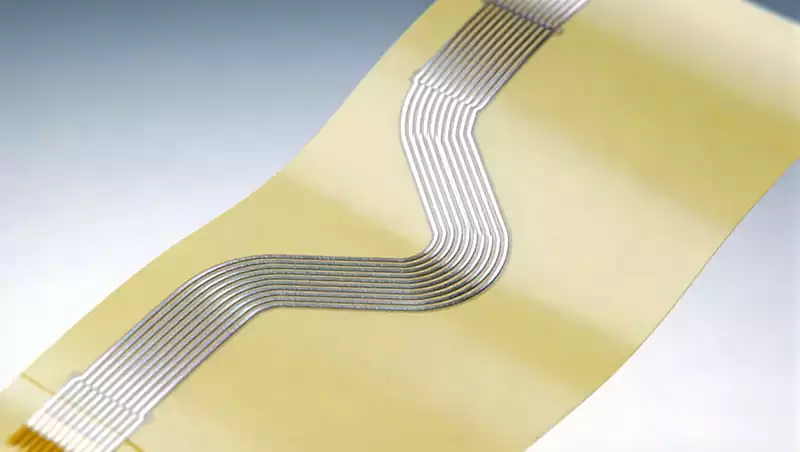
Multilayer PCB processing involves carefully laying out multiple layers of circuits on a single board and combining them through clever stacking and joining techniques. Compared to traditional single- or double-layer PCB designs, multilayer PCBs significantly increase wiring density and effectively reduce the size of the board, which in turn enhances overall performance and stability. This process not only improves the integration of electronic products, but also meets the market demand for efficient, compact and high-performance circuit boards.
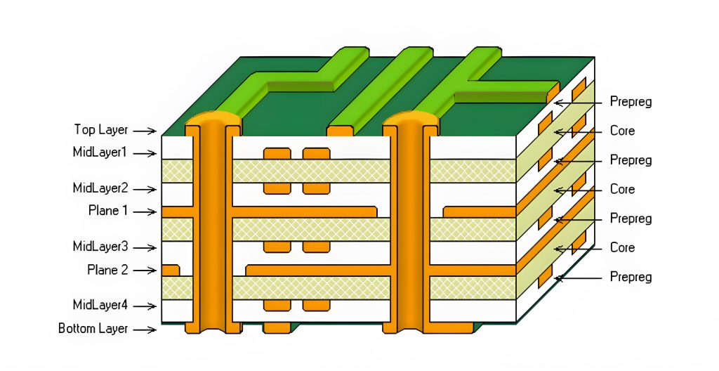
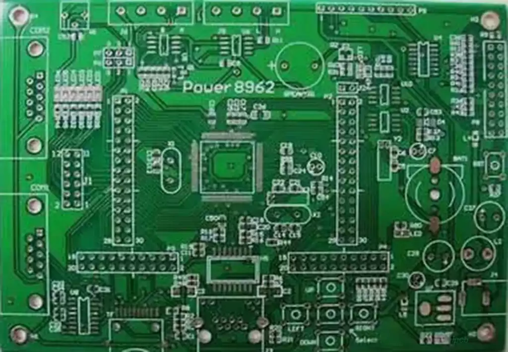
At the heart of board density optimization lies carefully planned layer stacking and circuit layout.
With the fine processing of multilayer PCBs, we can skillfully arrange the signal layer, ground layer and power layer, which have different functions, to be dispersed in each layer, so as to effectively avoid the interference and overlapping between the lines. At the same time, through the carefully designed interlayer connection scheme, we can make the circuit board wiring more compact, reduce the length of the line, and thus improve the efficiency and stability of signal transmission.
In addition, the multilayer PCB process also has the advantage of realizing a higher degree of component integration. In multilayer PCB design, we can use smaller packages and more compact layout strategy, more components integrated into the same circuit board. This not only significantly reduces the overall size, but also helps to reduce the number of connections between boards, thereby improving system reliability and immunity to interference.
However, to achieve the full optimization of circuit board density, simply relying on multi-layer PCB processing is not enough. In the design phase, we also need to carefully select components, optimize the wiring strategy, electromagnetic compatibility analysis. Only a comprehensive consideration and balance of these factors, we can truly optimize the density of the board, to enhance the performance of electronic products and enhance competitiveness to lay a solid foundation.
The high-density characteristics of HDI boards are mainly reflected in three key aspects: holes, lines and interlayer thickness.
First of all, small hole technology is an important part of the realization of high density. Especially when the hole diameter is less than 150mm, the requirements of micro-hole technology become extremely strict, which not only involves cost control and production efficiency, but also relates to the precise control of hole accuracy.
Secondly, the fineness of the line is also an important indicator of the high-density characteristics of the HDI board. This is mainly reflected in the increasingly stringent requirements for wire defects and wire surface roughness to ensure the stability and reliability of the line.
Finally, the reduction of dielectric thickness is also one of the key measures to achieve high density. As the interlayer dielectric thickness gradually converges to 80mm or even thinner, the requirements for thickness uniformity are increasingly stringent. This requirement is especially important for high density boards and package substrates that require characteristic impedance control.
PCB density is an important parameter in the field of electronics manufacturing, which needs to be fully optimized and weighed in the design phase. Through reasonable control it can meet the functional requirements of the product at the same time, improve production efficiency, reduce manufacturing costs, thereby enhancing the competitiveness of the product.