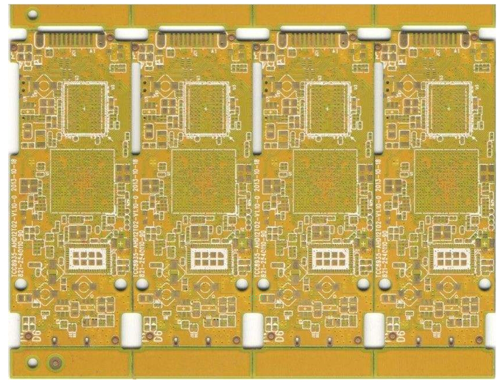
What is PCB design? PCB design is based on circuit schematics to achieve the functions required by circuit design engineers. Circuit board design mainly refers to layout design, which needs to consider the layout of external connections. Various factors such as optimized layout of internal electronic components, optimized layout of metal connections and through-holes, electromagnetic protection, thermal dissipation, etc. Excellent PCB design can save production costs and achieve good circuit performance and heat dissipation. Simple circuit design can be achieved manually, while complex PCB design requires the use of CAD.
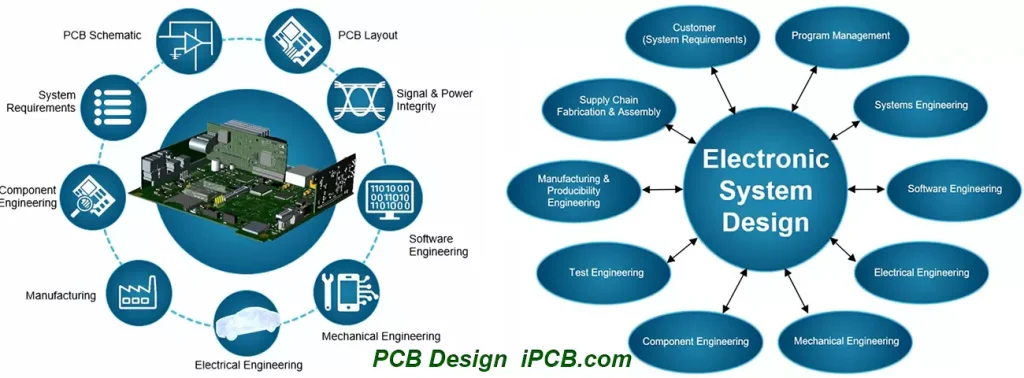
PCB design is the entire process of creating a PCB through collaboration and integration across multiple disciplines and fields, including electrical, mechanical, software, systems, testing, and manufacturing. This is a team work that requires continuous two-way communication.
PCB design steps
Design preparation: Clarify design goals and requirements, including the functionality, size, and cost of electronic devices, and select appropriate PCB substrate materials and components.
Circuit schematic design: Use circuit design software to draw a schematic diagram that includes all component symbols, pin connection relationships, and power and signal paths.
PCB layout: Consider the connection relationships between components, signal paths, power and ground layout, as well as the size, number of layers, aperture and other parameters of the PCB board, and place the components on the PCB board.
Cascade design and impedance control: Determine the position and thickness of each conductive layer, as well as the material and thickness of the insulation layer, and control the impedance characteristics of the transmission line by adjusting the width and spacing of the wires.
Wiring design: Connect component pins through wires to achieve the connection relationship in the circuit schematic, considering the width, length, and spacing of wires to meet the requirements of electrical performance and signal integrity.
Post processing and verification: including adding solder mask layer, silk screen layer and other process requirements, and conducting design rule checks and electrical rule checks to ensure that the design meets specifications and standards.

In PCB, special components refer to key components in the high-frequency part, core components in the circuit, components that are susceptible to interference, components with high voltage, components with high heat generation, and some heterosexual components. The position of these special components needs to be carefully analyzed, and the strip layout should meet the requirements of circuit function and production needs. Improper placement of them may result in circuit compatibility issues and signal integrity issues, leading to the failure of PCB design.
When placing special components in design, the first consideration is the size of the PCB. iPCB pointed out that when the PCB size is too large, the printing lines are long, the impedance increases, the anti drying ability decreases, and the cost also increases; When it is too small, the heat dissipation is not good, and the adjacent lines are easily disturbed. After determining the size of the PCB, determine the square position of the special components. Finally, layout all components of the circuit according to the functional units. The position of special components should generally follow the following principles when laying out:
- Try to shorten the connection between high-frequency components as much as possible, and try to reduce their distribution parameters and electromagnetic interference with each other. Components that are susceptible to interference should not be too close to each other, and input and output should be kept as far away as possible.
- Some components or wires may have a high potential difference, and their distance should be increased to avoid accidental short circuits caused by discharge. High voltage components should be placed out of reach of hands as much as possible.
- Components weighing over 15G can be fixed with brackets and then soldered. Those heavy and hot components should not be placed on the circuit board, but on the bottom plate of the main box, and heat dissipation should be considered. Thermal sensitive components should be kept away from heating components.
- The layout of adjustable components such as potentiometers, adjustable inductance coils, variable capacitors, microswitches, etc. should consider the structural requirements of the entire board. Some commonly used switches should be placed in a place that is easy to reach by hand if the structure allows. The layout of components should be balanced, with appropriate density, and should not be top-down.
The success of a product requires a focus on internal quality. The second is to balance the overall aesthetics, as only a PCB circuit board that is perfect for both can become a successful product.

Common PCB design software
PCB design engineers often use protels, protel 99se,protel DXP,Altium, These are all software that a company is developing and constantly upgrading. The current version is Altium Designer 15, which is relatively simple and has a more casual design, but when it comes to complex PCB designs, these software are not very user-friendly.
Cadence SPB software Cadence SPB is Cadence’s software, and the current version is Cadence SPB 16.5. The ORCAD schematic design is an international standard. The PCB design and simulation are very comprehensive, and it is more complex to use than Protel, mainly due to complex requirements and settings. But with well-designed regulations in place, the design is twice the result with half the effort and is clearly more powerful than protel.
Mentor’s BORDSTATION and EE, among which BORDSTATION is only suitable for UNIX systems and not designed for PCs, are used by fewer people. The current version of Mentor EE is Mentor EE 7.9 and Cadence spb, which belong to the same level of PCB design software. In some aspects, it is inferior to Cadence spb, and its strengths are cable and fly wires.
EAGLE Layout is the most widely used PCB design software in Europe.
Among these PCB design software, Cadence spb and MentorEE are the undisputed kings. If you are a beginner in PCB design, it is more friendly to Cadence SPB. It can help designers develop good design habits and ensure good circuit design quality.
Printed circuit boards (PCBs) are the core of electronic devices, and PCB design is the key to ensuring the normal operation of these devices. An excellent product must meet both design requirements and production processes. Standardize the relevant process parameters of circuit design, process design, and PCB design of products, so that the produced physical products meet the technical specifications requirements of producibility, testability, maintainability, etc., and build the advantages of product technology, technology, quality, and cost in the product design process.


