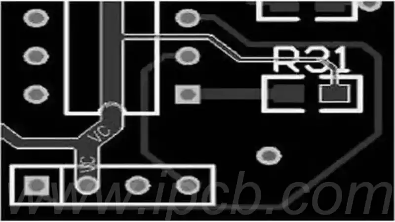
On a printed circuit board,board pitch refers to the distance between two pins or components,which is usually measured in millimetres. The correct layout of components is essential in the design of a circuit board.A smaller pitch means that the components are closer to each other,which makes the design more compact,but correspondingly more difficult to manufacture.Conversely,if the spacing is larger,there will be more space between the components,and although a larger board will be required,the assembly process will be easier.
Board pitch is an important determinant of equipment performance.The following guidelines should be followed during the design process:
Set the board pitch appropriately based on the specific functional requirements of the device. A board pitch that is too large or too small can have a negative impact on the performance of the device.
Take into account the layout and alignment of the components on the board during design to ensure that the set board spacing meets the necessary conditions for electrical connections between components.
Pay attention to the heat dissipation ability of the equipment, through the reasonable design of the board spacing to promote the effective transfer and dissemination of heat.
In PCB design, the main components of board pitch include:
Spacing between pins or leads: This refers to the distance between the centres of two adjacent pins or leads on a component.
Pin or Lead Diameter: This represents the specific size of the pins or leads of an electronic component. Typically, the thinner the pin or lead, the smaller the spacing required.
The size of the component: This covers the overall size of the component, in particular the distance between its outermost pins, and this dimension has a direct influence on the setting of the pitch.
Number of PCB layers: The number of layers in a PCB design also affects the pitch setting, as components may need to be spread over multiple layers to suit specific board size requirements.
Manufacturing tolerances: The manufacturing process of the PCB limits the minimum pitch that can be achieved. Therefore, the designer must take these manufacturing tolerances into account when planning the pitch.
Thermal considerations: The pitch setting also has an impact on the thermal performance of the board. To ensure good heat dissipation, the distance between components may need to be increased.
Electrical performance considerations: Spacing also has an impact on electrical performance, such as signal integrity and electromagnetic interference. Designers need to choose a pitch setting that properly balances electrical requirements and pitch challenges.
Steps to Success in Ensuring Proper PCB Design Spacing
1.Component Screening and Evaluation
Before PCB layout work begins, selecting appropriately sized components is critical to space utilisation. While smaller components can reduce footprint, they can drive up assembly costs, especially for grid-array ICs that require X-ray inspection. In some cases, it may be more cost-effective to select larger components to reduce costs. When designing a high-density PCB, component ratings should be weighed against package size to achieve the best margin and density balance. To maximise size and density benefits, it is recommended that capacitors maintain a margin of 20-30% and that priority be given to capacitors with 16V ratings.
2.Determine board specifications
After selecting the design and components for a high-density PCB assembly project, the first task is to determine the board size. Early in the project, environmental constraints (including dimensions in the X, Y, and Z directions) need to be considered. Connection interfaces, large components, and sensitive wiring need to be considered when assessing feasibility. Predefined board shapes, connection locations and 3D models help to determine the size and shape of the board before components are inserted.
3.Component Layout
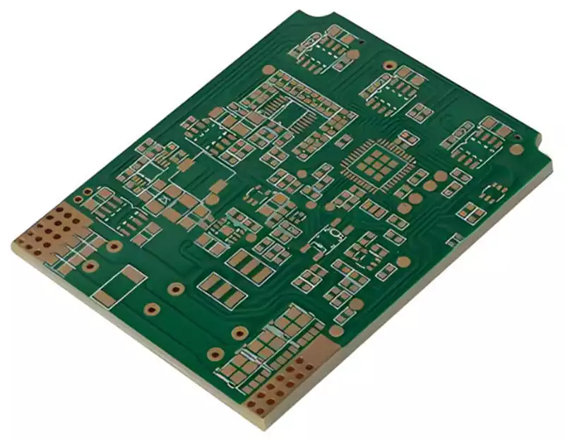
Once the design guidelines have been established, component layout can begin, ensuring that lines, vias and planes are unobstructed for maximum space efficiency. To frame the layout, high-power, high-speed connections and mechanical components are usually placed first. Where space is limited, as shown in the image of a fully populated board, screen printing is used only to show pin orientation and component outlines, as pick-and-place machines and procedures are sufficient to support assembly without additional indicators. Note that the X and Y dimensions of the board may change during the layout and routing process and may increase or decrease.
Strategies for optimising board pitch in fine pitch designs.
Introduce multilayer PCBs: In a fine-pitch design, components are tightly spaced and wiring needs to go through all components, taking up a lot of board space. The use of multilayer PCBs provides additional wiring layers that can significantly optimise space utilisation.
Accurate Component Layout: Designers need to layout components in an optimal way to maximise the use of available board pitch.Components should be placed in a way that reduces wiring distances and increases the space available between components.
Apply Via-in-pad technology: This technology frees up board space by creating via holes in the component pads. Through-holes can be created on each component to save wiring space.
Choose small components: In fine-pitch designs, small components can also be used to save space and reduce component density.
Optimise line width and spacing: Optimise line width and spacing by using thinner lines and reducing the space between lines. This helps to reduce wiring space and increase component density.
In the final stage of PCB design, it is critical to ensure that all board pitch settings meet both functional, manufacturing and assembly requirements. pitch optimisation in PCB design is a complex process involving multiple considerations, requiring in-depth expertise, hands-on experience and a meticulous work ethic on the part of the designer. As technology advances and manufacturing processes become more sophisticated, PCB design pitch optimisation will continue to be one of the key factors driving the miniaturisation and high performance of electronic devices.