An earthing layers, also known as a ground or shield layer, is a layer of circuit board design used to reduce electromagnetic interference, improve signal stability, and protect circuits from the external environment. It is usually located at the bottom of the board or in a specific area, and is connected to the grounding system of the equipment by forming a continuous conductive network through metal foils or conductive materials.
PCBs are usually composed of multiple layers of circuit boards, each of which has different functions and characteristics:
Signal Layer
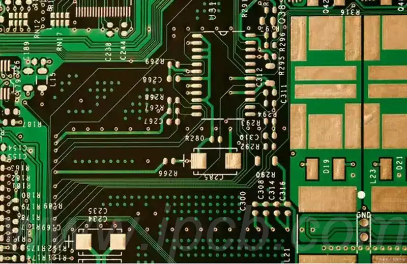
Signal layer is the most important layer in PCB board,it is the main layer connecting each component.On the signal layer, the circuit, signal transmission lines, power lines and grounding lines are usually arranged.The wiring design of the signal layer directly affects the performance and reliability of the entire PCB.
Power Layer
The power layer is a layer in the PCB substrate, which is mainly used to connect the power supply and the ground line.On the power layer,the power and ground lines are usually arranged to ensure that the power supply of the whole printed circuit board is stable and reliable.
Ground Layer
Ground layer is also a layer in the PCB substrate, which is mainly used to connect the ground of each component.On the Ground Layer,the ground and power lines are usually arranged to ensure that the ground connection of the whole PCB is stable and reliable.
Pad Layer
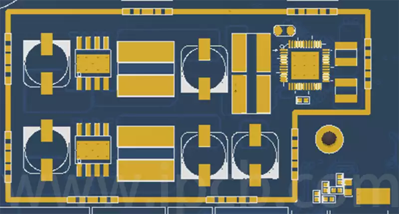
The pad layer is a layer in the PWB board, which is mainly used to connect the components and PCB board. On the pad layer, pads and jacks are usually arranged to enable components to be connected to the PCB plate.
Assembly Layer
The assembly layer is a layer in the circuit board, which is mainly used for assembling components.On the assembly layer,the mounting position and mounting method of the components are usually arranged so that the PCB manufacturer can assemble and solder the pcb components.
Solder Mask Layer
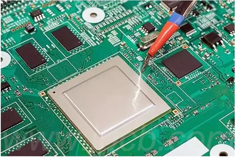
Solder Mask Layer is a layer in the printed circuit board, which is mainly used to prevent short-circuiting and poor soldering during the soldering process. On the solder mask layer, a green paint is usually applied to protect the PCB from chemical corrosion and mechanical damage.
Copper Cladding Layer (Copper Layer)
Copper cladding is a layer in a PCB that is used to provide circuit connections and support. On the copper cladding layer, circuits and signal transmission lines are usually arranged to ensure stable and reliable circuit connections throughout the circuit board.
The grounding layer serves three important purposes on a PCB:
- Voltage return: Most every component on the PCB will be connected to the power network and then the return voltage will be returned through the grounding network. On boards with only one or two layers, the ground network must usually be routed using a wider alignment. However, by dedicating an entire layer to the grounding layer of a multilayer board, the process of connecting each component to the grounding network can be simplified.
- Signal Return: Regular signals also need to be returned, and for high-speed designs, it is important to have a clear return path to ground. Without this clear return path, these signals can cause significant interference to the rest of the PCB.
- Reduce noise and interference: As signal speed increases, digital circuits will have more and more switching states. This can generate noise pulses through the grounding circuit, which can affect the rest of the circuit. A grounding layer with a large conductive area helps to minimize this interference because it has a lower impedance compared to a grounding grid routed through an alignment.
By carefully planning the earthing layer configuration of a multilayer board,PCB designers can use the grounding layer to help control the electrical performance of the board. By using a grounding layer between two active signal layers,crosstalk between signals on those layers can be eliminated.And signal integrity of high-speed transmission lines can be improved by ensuring an uninterrupted signal return path through the ground plane.Ground layers are also often connected to components that become hot to help dissipate heat.
The basic principles of PCB ground design
(1) Separate digital and analog ground. If there are both logic circuits and linear circuits on the circuit board,they should be separated as far as possible.Low-frequency circuit ground should try to use a single point of parallel ground, the actual wiring difficulties can be part of the series and then parallel ground.High-frequency circuits should be grounded in series with multiple points, the ground should be short and rent, high-frequency components around the grid-like large-area ground foil as far as possible.
(2) The ground wire should be as thick as possible. If the grounding wire with a very stringy line, the ground potential changes with the current, so that the noise performance is reduced. Therefore, the ground wire should be thickened so that it can pass three times the allowable current on the printed circuit board. If possible, the grounding wire should be above 2~3mm.
(3) The grounding line constitutes a closed loop circuit. Printed board consisting only of digital circuits, the grounding circuit cloth into a group loop mostly improves noise immunity.
In PCB design, the importance of the earthing layer is self-evident. It not only bears the burden of reducing electromagnetic interference and improving signal stability, but also protects the circuit board from external environmental interference. With the rapid development of modern electronic equipment, the ground protection layer of the requirements are increasingly high. Designers need to accurately control the layout of the ground protection layer, material selection and synergy with other layers to ensure the performance and reliability of the entire board.