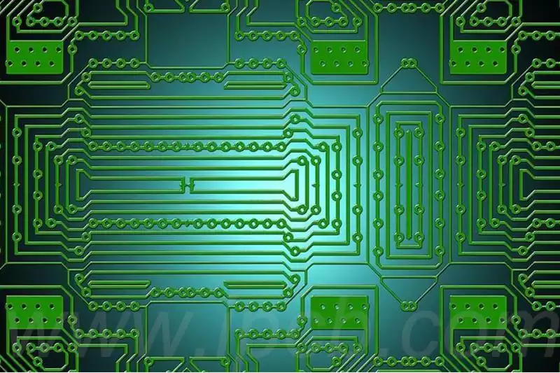
In the PCB circuit board printing process, the transformation of a bare board into a finished product with clear circuit graphics requires a series of sophisticated physical and chemical reactions, collectively known as pcb etching. Specifically, the process begins by pre-coating the outer layers of the board with a lead-tin alloy resist layer on the copper foil areas that need to be retained as circuit graphics to protect these critical parts from subsequent corrosion. Subsequently, the unprotected areas of copper foil are removed by chemical etching to bring out the complete circuit pattern. Currently, this process is commonly realised using the graphic plating method.
There are two main wet processes used by PCB manufacturers for circuit pattern etching:
- Acid etching (based on ferric chloride FeCl₃ or copper chloride CuCl₂)
Application Scenario:
Multilayer board inner layer circuit graphics production, pure tin substrate etching;
Suitable for ‘full-plate electroplating + dry film negative’ process.
Technical principle:
Selective removal of the unprotected copper layer by means of the chemical solubility of ferric or copper chloride.
Advantages of the process:
High precision: Acidic environment does not react with photoresist and can etch micron-sized lines accurately;
Low cost: material and equipment investment is lower than alkaline process;
Applicability: especially suitable for inner layer circuits, avoiding the problem of outer layer side etching (Undercutting).
Core formula:
Copper chloride, hydrochloric acid, sodium chloride or ammonium chloride.
Breakdown process:
Copper Chloride Etch: Mainstream choice for precise etching of minute features and support for low-cost continuous regeneration;
Ammoniated Copper System: copper hydride-sodium ammonia-hydrochloric acid (HCl) combination etches 1 ounce of copper in as little as 55 seconds at 130°F (~54.4°C) for fine-wire inner layer processing.
Ferric chloride etching:
Advantage: easy to work with, good retention of copper, suitable for screen inks, photoresists and gold patterns;
Limitations: not compatible with tin or tin/lead resist;
Solution Configuration: 28-42% by weight concentration, add up to 5% hydrochloric acid (HCl) to prevent precipitation.
safety requirements:
Copper chloride system needs to be equipped with chlorine leakage detection, emergency plan and professional protective equipment;
Ferric chloride solution needs to strictly monitor the concentration and acidity, and operators need to receive professional training. - Alkaline etching (based on ammonia)
Application Scenario:
Dedicated to PCB outer layer circuit etching.
Technical principle:
Remove the unprotected copper layer by chemical reaction between alkaline solution and copper.
Process Limitations:
Higher risk of side etching, parameters need to be optimised to reduce line edge loss.
Process Comparison and Selection
Acid etching:
Advantage: high precision, low cost, suitable for inner fine lines;
Disadvantage: longer time consuming, need to strictly control chemical concentration and time.
Alkaline etching:
Advantage: suitable for outer layer circuits, relatively simple process;
Disadvantage: significant side-etching problems, need to rely on late compensation technology.
PCB etching process principle
PCB etching is at a certain temperature conditions (45 +5) etching solution through the nozzle evenly sprayed to the surface of the copper foil, and no etching resist protection of copper redox reaction occurs, and the unwanted copper reaction off the exposure of the substrate and then stripped the film treatment to make the line shape. The main components of etching solution: copper chloride, hydrogen peroxide, hydrochloric acid, soft water (solubility has strict requirements)
PCB etching process quality requirements and control points
1. There can be no residual copper, especially double-sided panels should be noted.
2. There can be no residual glue, otherwise it will cause copper or plating adhesion bad.
3. Etching speed should be appropriate, do not allow the appearance of excessive etching and bowing line thinning, etching line width and total pitch should be the focus of control as this site.
4. Line welding point on the dry film shall not be flushed separation or fracture. 5, etching after stripping the film of the plate does not allow oil, impurities, copper skin soaring and other bad quality.
5. Put the board should pay attention to avoid card board, prevent oxidation.
6. Should ensure that the etching liquid distribution of uniformity, in order to avoid causing positive and negative or the same side of the different parts of the etching is not uniform.
PCB etching process should pay attention to the issue of
Reduce side pcb etching and edge
Side pcb etching will produce a protruding edge. Usually the longer the printed board is in the etching solution, the more serious the case of side-etching. Side-etching will seriously affect the accuracy of printed wires, and severe side-etching will make it impossible to make fine wires. When the side etching and abrupt edge is reduced, the etch factor will rise, and a high etch factor indicates that there is the ability to maintain a fine wire, so that the etched wire can be close to the size of the original drawing. Plating etchers, whether tin-lead alloy, tin, tin-nickel alloy, or nickel, can cause a short in the wire when the raised edge is excessive. This is because the protruding edge tends to tear down and create an electrical tear-off between two points of the wire.
Factors affecting side etching
1. Etching method: immersion and bubble etching will cause greater side corrosion, splash and spray etching side corrosion is smaller, especially spray etching the best results.
2. The type of etching solution: different etching solution, its chemical components are not the same, etching rate is not the same, etching coefficient is not the same. For example, acidic copper chloride etching solution etching coefficient is usually 3, and alkaline copper chloride etching coefficient can reach 4.
3. Etching rate: slow etching rate will cause serious side corrosion. Improve the quality of etching and speed up the etching rate has a great relationship, the faster the etching rate, the substrate in the etching of the shorter the stay, the side of the amount of corrosion will be smaller, etching out of the graphic will be more clear and neat.
4. Etching solution PH value: alkaline etching solution PH value is higher, side corrosion will increase. In order to reduce side corrosion, PH value should generally be controlled below 8.5.
5. The density of etching solution: alkaline etching solution density is too low will aggravate the side corrosion, the choice of high copper concentration of etching solution to reduce the side corrosion is very favourable.
6. Copper foil thickness: to achieve the minimum side corrosion of fine wire etching, it is best to use (super) thin copper foil. And the thinner the line width, the thinner the copper foil thickness should be. Because the thinner the copper foil in the etching solution will be the shorter the time, the smaller the amount of side corrosion.
PCB etching process refinement needs to balance technical precision and quality control, through process optimisation and defect suppression, to provide a reliable guarantee for the mass production of high-density circuit boards, and continue to promote the upgrading of electronic manufacturing technology.