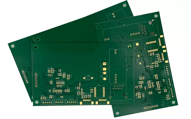
What is PCB Fabrication ? PCB Fabrication is the process of integrating electronic components, wires, and insulation materials onto a circuit substrate using various processes and technologies according to design requirements. This process involves multiple steps, including substrate selection, lamination, drilling, electroplating, etching, and welding. Through these complex processes, high-precision PCBs can be produced to meet the needs of various electronic products.
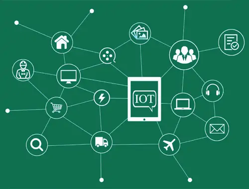
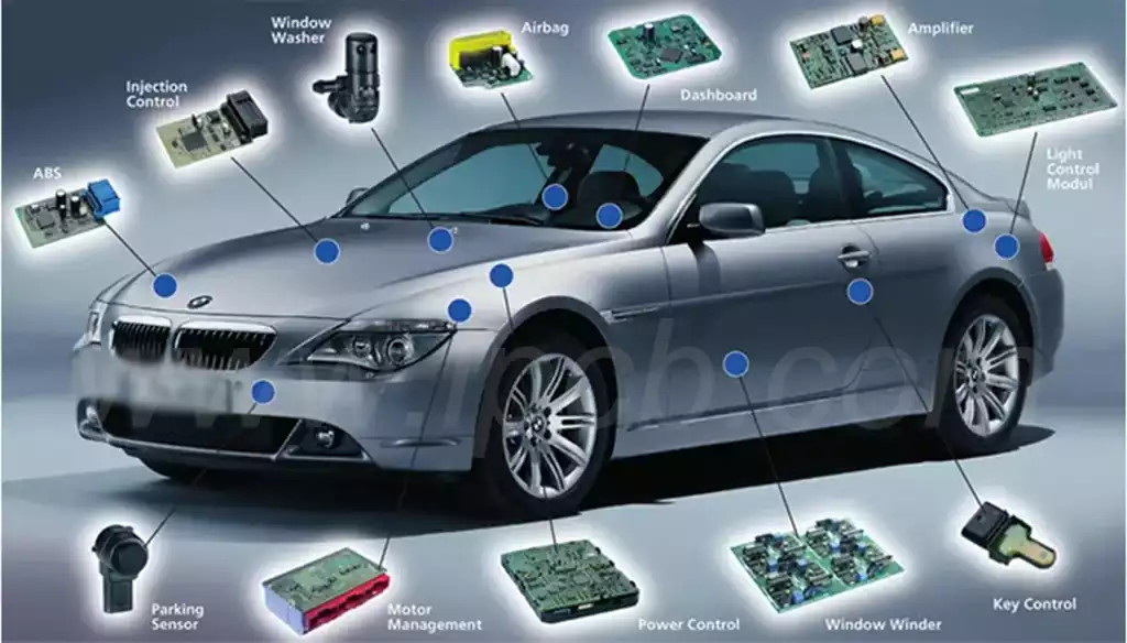
PCB circuit boards are widely used in almost all electronic products, from watches and earphones to military and aerospace industries. With the rapid development of technology, electronic products have become an indispensable part of our daily lives, and PCB Fabrication is an important component of electronic manufacturing.
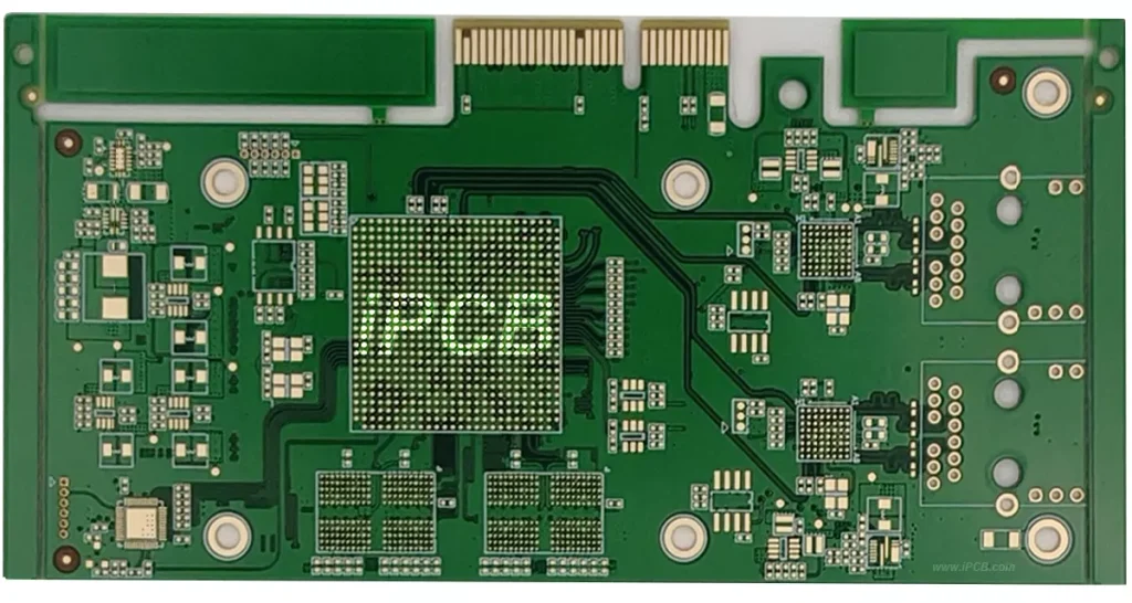
PCB Fabrication Process Flow
The process flow of double-sided PCB Fabrication : cutting ->drilling ->perforation and full board electroplating ->pattern transfer (film formation, exposure, development) ->etching and stripping ->solder mask and characters ->HAL or OSP, etc. ->external processing ->inspection ->finished product
Process flow of multi-layer PCB Fabrication : cutting ->inner layer production ->oxidation treatment ->lamination ->drilling ->hole electroplating (can be divided into full board and graphic electroplating) ->outer layer production ->surface coating ->external processing ->inspection ->finished product
Inner layer production refers to the process of in process board production after cutting ->pattern transfer (film formation, exposure, development) ->etching and film removal ->inspection, etc.
Outer layer production refers to the process of electroplated perforated boards, pattern transfer (film formation, exposure, development), etching, and film removal.
Surface coating (plating) refers to the production of the outer layer ->solder mask and characters ->coating (plating) layer (such as HAL, OSP, chemical Ni/Au, chemical Ag, chemical Sn, etc.).
The process flow of buried/blind hole PCB Fabrication : cutting ->forming a core board (equivalent to conventional double-sided or multi-layer boards) ->lamination ->the following process is the same as conventional multi-layer boards.
Forming a core board refers to the process of forming double-sided or multi-layer boards using conventional methods, and then forming buried/blind hole multi-layer boards according to structural requirements. If the thickness to diameter ratio of the holes in the core board is large, plugging treatment should be carried out to ensure its reliability.
HDI PCB Fabrication Process
Core board production ->Laminated RCC ->Laser drilling ->Holing electroplating ->Pattern transfer ->Etching and film removal ->Laminated RCC ->Repeatedly forming an integrated printed board (HDI/BUM board) with a+n+b structure.
The core board here refers to various types of boards, such as conventional double-sided, multi-layer boards, buried/blind hole multi-layer boards, and so on. But these core boards must be blocked and surface polished before they can be laminated.
The multi-layer board structure of HDI PCB can be represented by the following equation. A+n+b, where a is the number of layers on one side, n is the core board, and b is the number of layers on the other side.
Common equipment for PCB Fabrication : cutting machine, circuit exposure machine, etching line, drilling machine, electroplating line, solder mask printing machine, optical inspection machine, browning line, fully automatic laminating machine, forming machine, electrical testing machine, sinking gold production line
The acceptable PCB Fabrication file formats for iPCB include Gerber files, cam files, DXF files, PCBDOC files, CAD files, PCB files, BRD files, and pcbddb files.
PCB file format description. Currently, the most common CAD design software is PCAD, Protel,Allegro,PADS,OrCAD,AutoCAD
. pcb: The most common suffix, which is used in many PCB design files, including Protel and PADS. In addition, it also includes ZUKEN’s Cadstar, CR5000, Altium’s P-CAD, etc. The suffix is PCB’s gerber file, which can be opened with CAM350.
. brd. Cadence Allegro, Eagle
Another PCB design software ORCAD from. max. cadence company
Text file output by. min. ORCAD
. pcbdoc. Protel New Version DXP, AD6 Design
. asc Text formats for some PCB software, such as PADS, protel, P-cad, etc
. dat,. neu,. net, etc. The netrual file generated by Mentor
. cam. CAM350 or Camtastic 2000 files
. ODB++files generated from. tgz. PCB design files
. Gencad files generated from. cad. PCB design files
Some formats are not in the form of files, but in the form of folders. One of them is the central library, which is a mentor expedited design file
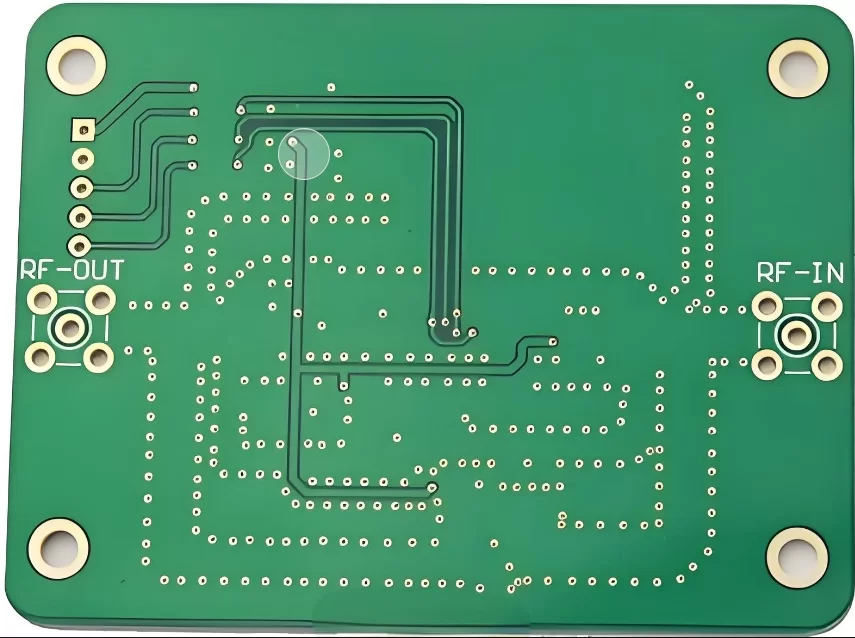
PCB Fabrication needs to provide: Gerber flies, PCB board making process requirements (board thickness, copper thickness, solder mask color, silk screen color, surface treatment process), impedance printed circuit boards need to provide impedance values.
Before PCB Fabrication , it is necessary to evaluate:
1. Is Gerber flights complete and complete? Specific information such as PCB Fabrication process requirements, impedance control requirements, etc.
2. Whether the PCB process capability meets the design requirements, including producibility, electrical testing, and maintainability.
After the PCB Fabrication is completed, iPCB can provide customers with processed Gerber flies, steel mesh files, panel files, impedance test reports, and PCB slice analysis reports.
The delivery time for fast PCB sample fabrication supported by iPCB is:
Single/double-sided PCB delivery time: 3-4 days
Delivery time for four layer PCB: 5-6 days
Six layer PCB delivery time: 7-8 days
iPCB Company mainly produces microwave high frequency PCBs, high frequency mixed voltage, ultra-high multi layer IC testing, HDI PCBs, any layer HDI PCB, IC substrate, IC test board, rigid flexible PCB, and ordered multi layer FR4 PCBs. If you need PCB Fabrication, please consult iPCB.