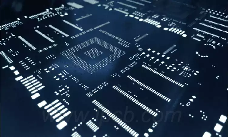
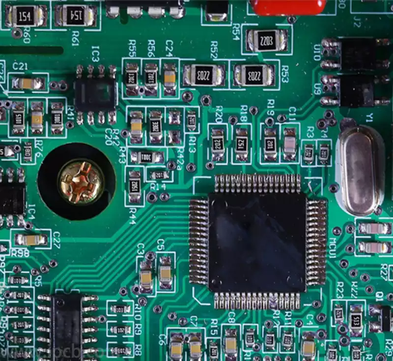
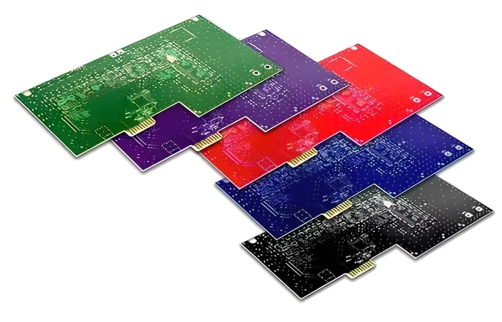
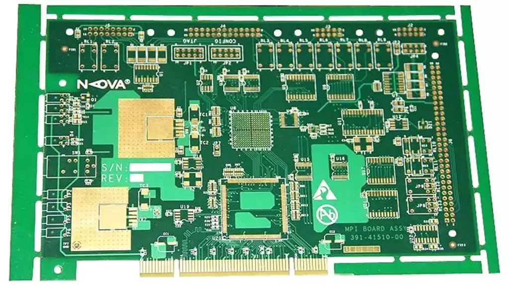
PCB Gold Finger, as a key component of a printed circuit board, refers to the gold-plated conductive posts that connect the edges. Its central role is to ensure that the auxiliary PCB can be smoothly connected to the computer motherboard or other devices to achieve accurate signal transmission. Whether it’s a smartphone, smartwatch or other digital device, PCB gold fingers play an integral role. Because gold has excellent conductive properties, it is often used as a connection point for PCBs to ensure the smooth flow of current.
According to the design and application requirements, PCB gold finger can be divided into three main types:
Ordinary PCB Gold Finger: This type of Gold Finger has a horizontal and uniform array structure, pad length, width and spacing are consistent, is the most common type of Gold Finger.
Non-uniform PCB Gold Finger: This type of Gold Finger has the same pad width, but with differences in length or spacing. In some specific applications, such as memory card readers, some fingers are designed to be shorter than others to meet specific electrical connection requirements.
Segmented PCB Gold Fingers: The pad lengths vary and some of the fingers are even segmented within the same circuit board. This design is common in electronic products that require waterproof or ruggedized performance.
Plating is a key step in the production of gold fingers. The following are the two main plating methods:
Electroless Nickel Immersion Gold (ENIG): This method is more cost-effective than electroplating and offers better solderability. However, due to its soft and thin nature, it is not suitable for PCB gold fingers that are frequently inserted and removed or subjected to high wear and tear.
Hard Gold Plating: Hard gold is solid and thick, making it more suitable for PCB fingers that are subjected to constant wear and tear.
The presence of gold fingers allows different circuit boards to communicate with each other. From the power supply to the device, the transmission of signals relies on the connection between multiple contacts to ensure the accurate execution of commands.
The process of plating hard gold usually includes the following steps:
Cover all but the PCB gold finger pads to be plated with blue glue, ensuring that the conductive location is in the same orientation as the board.
Remove the oxide layer on the copper surface of the PCB board pads and further clean the surface by grinding.
Plate a layer of nickel on the cleaned gold finger pad surface.
Plate a layer of gold on the nickel-plated PCB pad surface and recover the remaining gold.
Remove the bluing to complete the hard gold plating process of the gold finger and continue with the subsequent PCB manufacturing steps.
In practical applications, PCB gold fingers mainly perform the following functions:
As an edge connector, gold finger realizes the connection with motherboard or other devices by inserting into the female slot to ensure the smooth transmission of signals.
Through special adapters, gold fingers can enhance the performance of computers, such as providing enhanced graphics processing and high-fidelity sound.
In terms of external connections, gold fingers enable peripheral devices such as speakers, monitors, etc. to be connected to the computer motherboard for data interaction and transmission.
When designing PCB gold fingers, the following factors need to be considered:
Plated through-holes should be located away from the gold fingers to avoid potential interference and damage.
Gold fingers should be chamfered, generally at an angle of 45°, to ensure smooth insertion and removal and to minimize wear.
The surface of the gold finger needs to be treated with a full piece of soldermask windowing and avoid laying copper on the surface of the gold finger.
Inside the gold finger, all layers need to be copper cut to minimize impedance differences and improve ESD performance.
As an important part of printed circuit boards, PCB gold fingers play a key role in the communication and connection of electronic devices. Through reasonable classification, plating process design and usage methods, the performance and reliability of gold fingers can be ensured to meet the needs of various application scenarios.