PCB lamination is a process in which multiple layers of copper foil and insulation are compressed into a single unit by means of processes such as hot pressing and chemical reactions. It is an important step in the construction of a printed circuit board (PCB) and is used to ensure that the copper does not unintentionally conduct current or send signals. The lamination process consists of three stages: kiss pressing, full pressing and cold pressing. In the kiss-press stage, the resin moistens the bonding surface and fills the voids in the circuit, and then moves on to the full-press stage, which bonds all the voids. Cold pressing cools the board quickly and keeps it dimensionally stable. The entire process ensures the PCB board’s layer count, performance and reliability.
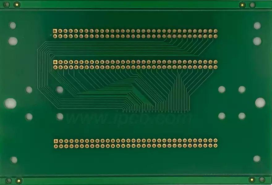
The PCB, or printed circuit board, is the core component that connects and supports electronic components. It interconnects components through conductive paths. These conductive paths are formed by etching copper sheets on the circuit board. To ensure that the copper layer carries signals or currents without problems, it must be securely laminated into the substrate.
Types of PCB lamination processes
The lamination process for PCBs depends on the type of board used, here are a few common methods of lamination:
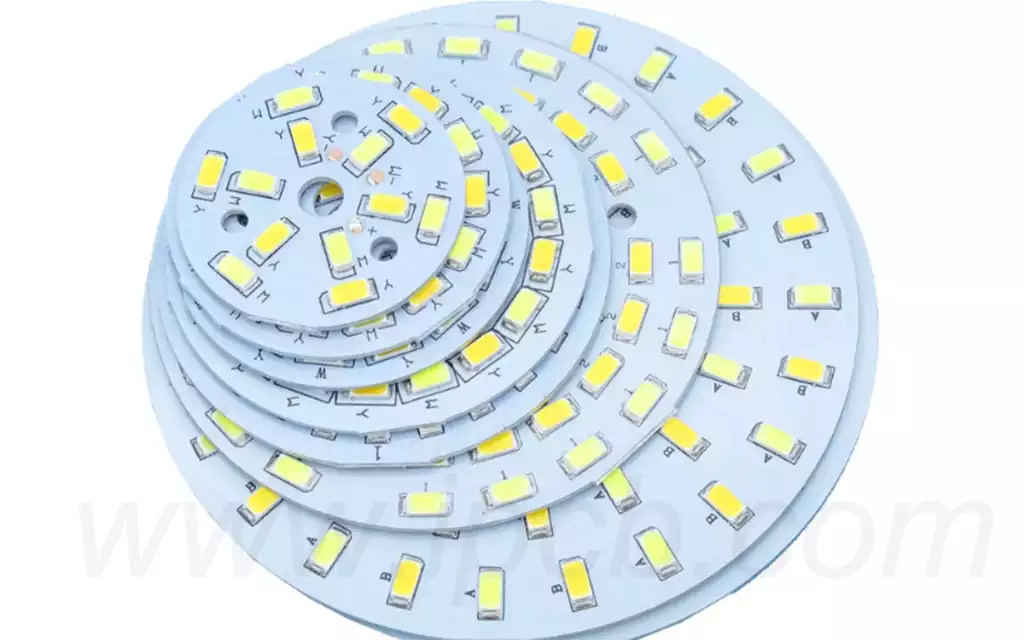
Multilayer PCB: A circuit board consisting of multiple layers is known as a multilayer PCB. These layers can be thin etched or wired layers which are tightly bonded together by lamination techniques. During the lamination process, the inner layers of the PCB are subjected to high temperatures (375°F) and high pressures (275 to 400 psi). This step is especially important when laminating with photosensitive dry resists. The PCB is then cured at high temperatures, followed by a slow pressure release and cooling.
Double-sided PCBs: Although the manufacturing process for double sided PCB is different from other types of circuit boards, the lamination technique is similar to that for multilayer PCBs. The same photosensitive dry resist layers are used for lamination.
Sequential Lamination: Sequential lamination technique is used when the PCB board contains multiple subsets. These subsets are created in a separate process and dielectric material is inserted between each pair of subsets.
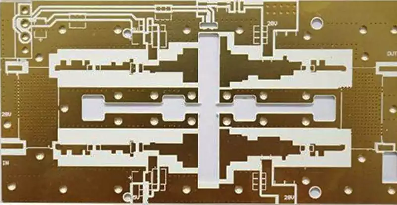
Polytetrafluoroethylene PCB (PTFE) Microwave Laminates: PTFE microwave laminates are commonly used in PCB lamination due to their consistent dielectric constants, extremely low electrical losses and tight thickness tolerances. It is especially suitable for RF and other applications.
Key considerations in the PCB prototyping process.
Number of samples: Before mass production, companies usually need to make a batch of PCB samples for testing. This increases the cost of the enterprise, especially when producing multiple types of PCB boards. Therefore, companies should carefully consider the number of samples in the PCB sampling process.
Device Packaging Inspection: Soldering a chip with a specific function onto a circuit board and packaging it with a shield is a critical step in the manufacturing process. During the proofing process, the client should pay close attention to whether the internal chips and electronic components are soldered correctly to ensure the quality of PCB proofing.
Comprehensive electrical inspection: After the proofing is completed, the company should carry out a comprehensive electrical inspection to ensure that every function and detail of the PCB has been examined. This is a key step to ensure that subsequent mass production can proceed smoothly and reduce the defect rate.
With the rapid development of electronic technology, PCB board sampling has become an important part of ensuring product quality and subsequent production. Taking every aspect of the PCB lamination and proofing process seriously is the key to ensuring product quality and technological competitiveness.