What is PCB Layout? PCB Layout refers to the layout design of a PCB board, which is the process of converting a circuit diagram into a physical layout of a PCB. In the design process, it is necessary to arrange and connect components, signal lines, power lines, ground and other elements reasonably according to the requirements of the circuit diagram, in order to achieve correct and stable operation of the circuit.
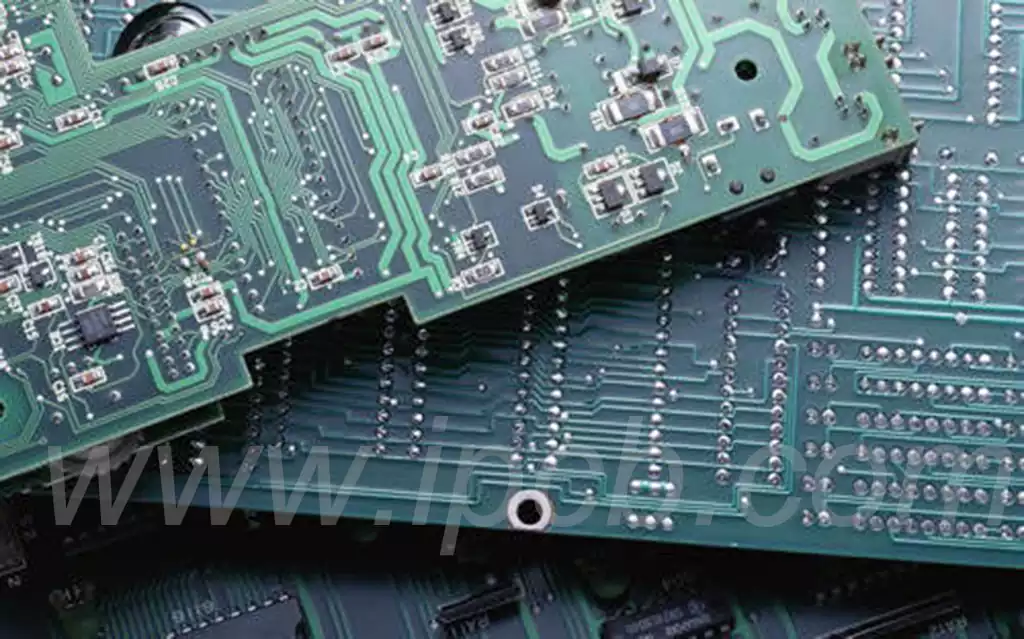
PCB layout is a method of using printing and etching to create circuits on a circuit board. Before the emergence of PCBs, electronic components were connected through wires, which not only were intricate and disorderly, but also posed safety risks. At the heart of electronic devices such as printed circuit boards, PCB layout is undoubtedly a crucial nervous system. It achieves stable and efficient connections and information transmission through carefully designed wiring and PCB components.
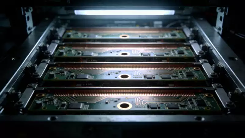
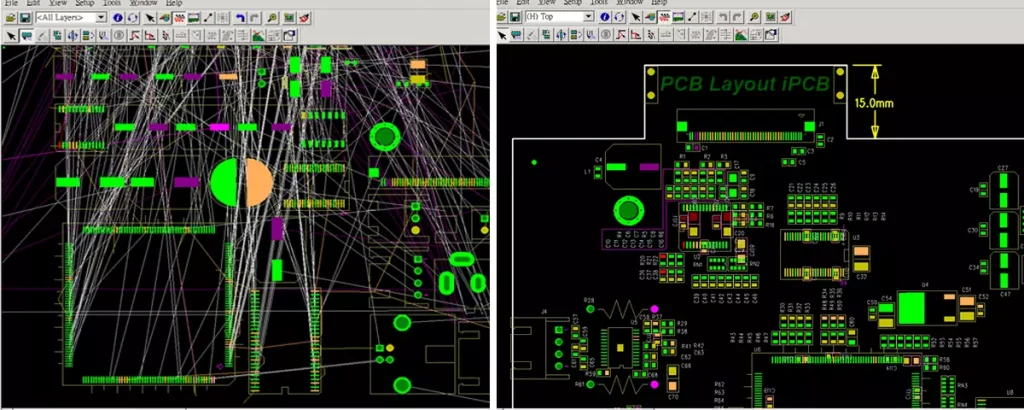
PCB design needs to be implemented through computer design. Common design software used by PCB layout engineers include Cadence Allegro, PADS, Altium Designer, etc.
The conventional PCB layout design includes several steps such as library building, grid adjustment, layout, wiring, and file output, but the conventional PCB layout design process is far from meeting the increasingly complex high-speed PCB design requirements.
Due to the close integration of SI simulation, PI simulation, EMC design, and single board process into the design process, as well as the need to add review processes at each node to achieve quality control, the actual PCB layout design process is much more complex.
Driven by Moore’s Law, the electronic industry is experiencing stronger product functionality, higher integration, faster signal rates, and shorter product development cycles. Due to the continuous miniaturization, precision, and high-speed of electronic products, PCB layout design not only needs to complete the wiring connections of various components, but also needs to consider the various challenges brought by high speed and high density.
PCB layout design is no longer a subsidiary of hardware development, but has become an important part of front-end IC, back-end PCB, and SE integration in product hardware development.
System engineers complete IC selection and function definition based on product functional requirements, and develop schematic diagrams according to IC company’s principle reference design. The work of traditional hardware engineers in circuit development is gradually decreasing, and circuit development work is gradually shifting towards IC engineers and PCB layout engineers.
PCB engineers, based on the principle scheme provided by the system engineer and with the cooperation of the structural engineer, complete the PCB design according to the current processing technology and capabilities of the PCB factory while considering SI, PI, EMI, structure, and heat dissipation as a whole.
PCB layout is the channel for current and signal transmission in electronic devices. It connects components to ensure stable current transmission and accurate signal transmission. The carefully designed wiring not only improves the electrical performance of the equipment, but also enhances its anti-interference ability, allowing the equipment to operate stably in complex operating environments.
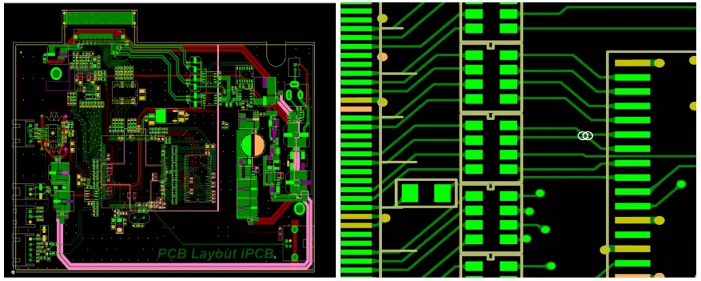
During the PCB layout process, there are two key elements that require special attention. Firstly, the length of the wiring. The moderate length ensures the normal transmission of signals and avoids delays. Excessive wiring may cause signal delay and affect device performance. Short wiring may increase signal attenuation and even cause electromagnetic interference (EMI) problems.
Next is the width of the wiring. An appropriate width can ensure stable current transmission, prevent overheating and voltage drop. Engineers need to choose the wiring width reasonably based on the current size and transmission speed requirements. Excessive width may cause line heating and signal distortion. Being too narrow may lead to space travel and waste of space.
In addition, the layout and direction of PCB also greatly affect performance. Correct alignment and direction can reduce mutual interference between signals and improve equipment stability. To achieve this goal, engineers use layered design, grounding shielding, and other means to reduce the impact of electromagnetic interference and signal coupling. These technologies help reduce mutual interference between signals, improve the anti-interference ability and stability of equipment.
In special circumstances, such as high-precision or high-frequency electronic devices, the layout requirements are more stringent. These devices typically require finer line widths, straighter lines, rounder curves, etc. to minimize signal loss and reflection, and improve signal quality. In addition, in high-density and highly integrated printed circuit boards, wiring also needs to consider factors such as heat dissipation and electromagnetic shielding to ensure the reliability and stability of the equipment.
With the rapid development of science and technology, printed circuit board wiring technology is also constantly innovating. The emergence of new wiring materials, PCB layout tools, and simulation software has provided engineers with more design freedom and possibilities. Through advanced wiring technology, engineers can more efficiently complete designs, improve equipment performance and reliability. For example, advanced PCB layout software can simulate and analyze signal transmission characteristics, helping engineers predict and optimize circuit parameters. The new wiring material has better conductivity and mechanical properties, improving the transmission speed and stability of the line.
As the nervous system of electronic devices, the importance of printed circuit board wiring is self-evident. Excellent wiring design can make the performance of electronic devices more stable and reliable. On the contrary, poor wiring may lead to equipment malfunctions, signal interference, and other issues.
PCB layout should meet the following requirements as much as possible: the overall wiring should be as short as possible, and the key signal lines should be as short as possible. High voltage and high current signals are completely separated from weak signals of low voltage and low current signals. Separate analog signals from digital signals. Separate high-frequency signals from low-frequency signals. The spacing between high-frequency components should be sufficient. Local adjustments are made while meeting the requirements of simulation and timing analysis.
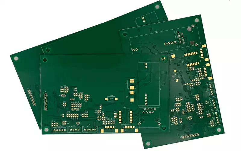
PCB layout design is the first important design step in the entire PCB design process. The more complex the PCB board, the better the layout can directly affect the difficulty of later wiring implementation.