When designing a printed circuit board (PCB), following basic pcb layout rules is essential to ensure the functionality and performance of the circuit.
The basic rules of PCB layout:
1.According to the layout strategy of ‘major priority, complexity first’, i.e., the key unit circuits and core components should be arranged first.
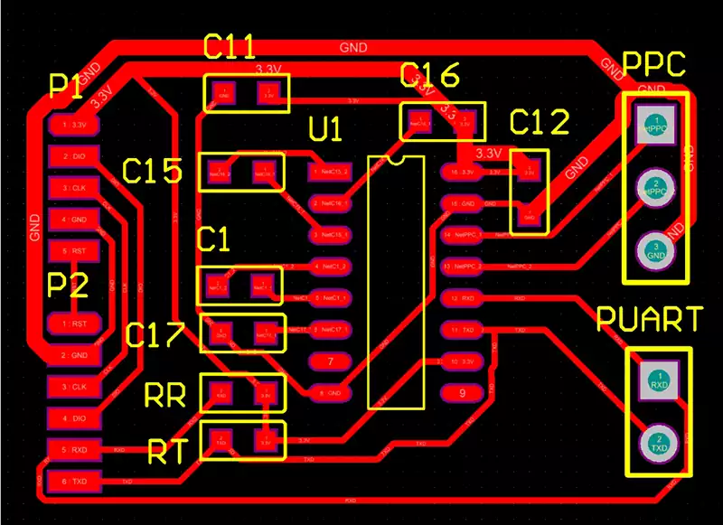
2.In the layout process, should refer to the schematic diagram, according to the main signal flow direction of the single board reasonable layout of the main components.
3.Layout design should meet the following alignment guidelines as far as possible: ensure that the key signal lines (such as ADC) is the shortest; high-voltage, high-current signals and low-voltage,low-current signals are completely isolated;analogue signals and digital signals are separately laid out; high-frequency signals and low-frequency signals are arranged separately;and high-frequency components to maintain sufficient spacing (such as inductance, etc.).
4.For the same structure of the circuit part,should try to use the ‘symmetrical’ standard layout.
5.Optimise the layout according to the criteria of even distribution,balanced centre of gravity and beautiful pcb layout. If there are special layout requirements, they should be communicated with the hardware team and determined.
6.Plug-in components of the same type should be placed in the same direction in the X or Y direction.Similarly,discrete components of the same type with polarity should be placed in the same direction in the X or Y direction as far as possible, so as to facilitate production and inspection.
7.Heat generating components should be evenly distributed to promote heat dissipation of the veneer and the whole machine. In addition to temperature detection components,temperature-sensitive devices should be away from the components of the heat.
8.Components should be arranged to facilitate debugging and maintenance, that is, small components should not be placed around the large components, debugging components should be left around enough space.
9.The distance between the outside of the pad of the SMD component and the outside of the adjacent inserted component should be greater than 2mm, and the distance between other SMD components should be greater than 0.7mm.
10.The layout of IC decoupling capacitors should be as close as possible to the IC’s power supply pins,and ensure that the shortest circuit is formed between it and the power supply and ground.
11.In the layout of components,due consideration should be given to the use of the same power supply devices together in order to facilitate future power separation.
12.For complex circuit boards,the layout can be sent to the hardware team for checking after completing the layout,and then wired after making modifications based on the feedback.

In the layout design of the PCB, the layout of components plays a crucial role,which is not only related to the neatness and beauty of the board,but also has a direct impact on the length and number of printed wires, which will have a certain impact on the reliability of the machine.
Component layout of the basic principles
1.PCB Layout in accordance with the circuit module to achieve the same function of the circuit as a module,the components within the module should follow the principle of proximity and concentration of the layout, and to ensure that the digital and analogue circuits are separated from each other;
2.Prohibit the mounting of components within 1.27mm of non-mounting holes such as positioning holes and standard holes, and within 3.5mm (for M2.5 screws) or 4mm (for M3 screws) of mounting holes such as screws;
3.In the horizontal mounting resistors, inductors (plug-in), electrolytic capacitors and other components below, should avoid the layout of the over-hole, in order to prevent short-circuiting after wave soldering over-hole and component shells;
4.The distance between the outer edge of the component and the edge of the board should be maintained for 5mm;
5.The distance between the outer edge of the pad of the mounted component and the outer edge of the adjacent inserted component should be greater than 2mm;
6.Metal shell components and metal parts (such as shielding box, etc.) should avoid contact with other components,and can not be close to the printed line or pad, the distance should be greater than 2mm. positioning holes, fastener mounting holes, elliptical holes and other square holes in the board should be greater than the distance between the outer edges of the board edge and 3mm;
7.Heat-generating elements should be avoided in close proximity to wires and thermal components,high heat devices should be balanced distribution on the entire board;
8.Power sockets should be arranged as far as possible around the printed circuit board, and power sockets and their connected bus bar terminals should be arranged on the same side. Special care should be taken to avoid arranging power sockets and other soldering connectors between the connectors to facilitate the soldering of these sockets and connectors as well as the design and fixing of power cables.Power socket and welding connector layout spacing should be considered to facilitate the plugging and unplugging of the power plug;
9.Layout of other components:all IC components should be aligned on one side,the polarity of the polarity components should be clearly and consistently marked, the same printed circuit board should not be more than two directions of the polarity marking,if there are two directions, the two directions should be perpendicular to each other;
10.Board wiring should be sparse and moderate, when the difference between sparse and dense,should be filled with mesh copper foil, grid size should be greater than 8mil (or 0.2mm);
11.SMD pads should not have through holes to prevent the loss of solder paste resulting in component soldering.Important signal lines should be avoided from the socket between the feet through;
12.SMD components should be aligned on one side, with the same character direction,and the package direction should also be consistent;
13.On the same board, the polarity of the devices with polarity labelling direction should be as consistent as possible.
PCB layout rules are the cornerstone of ensuring board performance and reliability. By following these rules and combining them with practical experience, designers can create both efficient and aesthetically pleasing circuit boards that meet the stringent requirements of modern electronic products.


