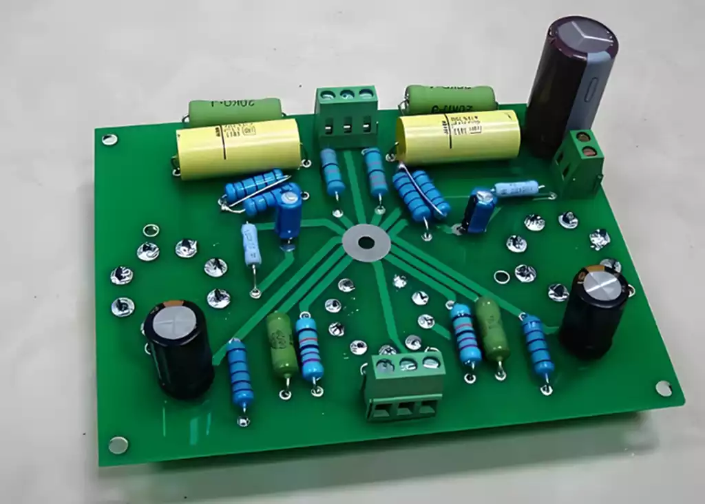
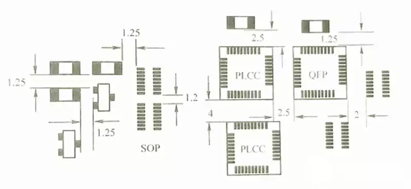
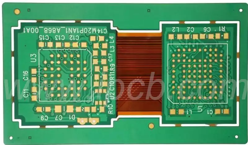
In PCB design,pads as a bridge connecting components and circuit boards, its type and design standards are critical. Different types of pcb pads are suitable for different components and application scenarios, while reasonable design standards ensure soldering reliability and board performance.
Common pcb pad types:
Square pads: suitable for large and small number of components, as well as simple printed wire layout. Easy to make when making PCBs by hand.
Round pads: Widely used in regular arrangement of single and double-sided printed circuit boards. If the board surface allows, the pads can be designed slightly larger to ensure solid soldering.
Island-shaped pads: fusion of lines between the pads, suitable for vertical irregular arrangement of components installed.
Polygonal pads: Used to differentiate pads with similar outside diameters but different hole diameters for ease of processing and assembly.
Oval pads: Enhance peeling resistance, commonly used for dual-row in-line devices.
Open pads: Ensure that pad holes are not sealed by solder after wave soldering for manual patching.
Special pcb pad types:
Plum Blossom Pad: Used for large over-hole grounding to prevent reflow from clogging the holes and to ensure good grounding.
Cruciform pads: Reduce soldering heat dissipation, prevent false soldering or PCB skinning, suitable for ground and reflow.
Tear drop pads: used for fine alignment connection, prevent pcb pad skinning and alignment disconnection, commonly used in high frequency circuits.
Design Standards:

Call the standard package library.
The pad is not less than 0.25mm on one side, and the diameter is not more than 3 times the hole diameter.
Pad spacing greater than 0.4mm.
Large aperture or pad using diamond or plum blossom shape.
Dense wiring using oval or oblong pads.
Hole in the pcb pad is not less than 0.6mm, usually the hole diameter plus 0.2mm.
Reliability design points:
Symmetry: Ensure that the surface tension of the molten solder is balanced.
Pad spacing: Proper spacing to avoid soldering defects.
Residual size: Ensure that the solder joints form a curved moon face.
Pad width: consistent with the component end or pin width.
The type and design criteria of PCB pads have a significant impact on the reliability and performance of the board.By choosing the right type of pad and following the design standards, you can ensure a solid connection between the components and the circuit board to improve soldering quality and productivity. Therefore, in the PCB design process, the design of the pads should be fully considered to ensure the stability and reliability of the circuit board.
