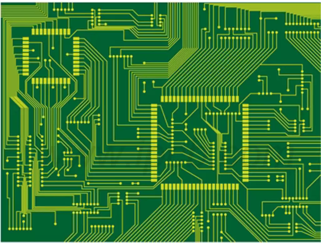
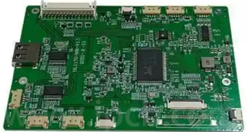
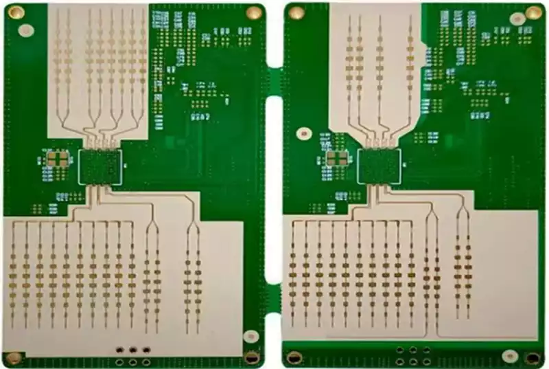
A PCB radar is a type of printed circuit board designed for use in radar systems and is primarily responsible for generating, transmitting and receiving RF signals. It is typically made of a high frequency laminate material that integrates an antenna structure for transmitting and receiving radar waves. The radar PCB is able to send out the emitted radio waves, and when these waves meet objects and reflect back, the PCB then receives and analyses the reflected signals through RF circuits, thus achieving detection, positioning and speed measurement of the target. As radar systems operate in the high frequency range (generally from 1 GHz to 77 GHz or even higher), radar PCBs require a high degree of attention to signal integrity, electromagnetic compatibility, and low-loss material properties during the design and manufacturing process to ensure accurate transmission and stable performance of the radar signal.
Basic components of a PCB radar:
Transmitter: The radar cannot operate with weak signals from a waveform generator. Therefore, the function of the transmitter is to boost the signal using a power amplifier.
Receiver: The receiver uses a receiver processor (e.g. super-aberration) to find and analyse the reflected signal.
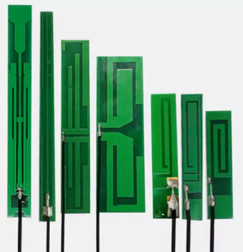
Antenna: Equipped with a phased array, planar array or parabolic reflector. It is responsible for sending and receiving pulses.
Duplexer: An electronic device called a duplexer allows two-way (duplex) communication over a single path. It separates the receiver from the transmitter in radar and radio communication systems so that they can share a common antenna. An antenna can be used as a transmitter and a receiver with a duplexer.
Waveguide: Data is transmitted over a transmission line in any pattern. When information is transmitted in the form of waves, these transmission lines are also called waveguides. On a pcb radar, these waveguides are used as transmission lines for transmitting signals and as paths for receiving signals.
Threshold Determination: When designing a circuit for any signal receiver, there will be a circuit to detect noise. In music, noise is considered to be sound below a specific frequency and is considered to be pollution. This component compares the output of the receiver with a threshold value to assess whether the object is present or not. After the comparison, if it operates below that point, noise can be inferred.
As with all RF and microwave PCBs, PCB materials have a critical impact on their electrical, thermal, and mechanical properties, as well as their cost and manufacturing process. Several laminate materials are commonly used in PCB radar:
RO4350B – One of the most popular materials for high-speed applications, RO4350B is recognised as one of the most popular materials in the market due to its good availability, excellent performance and reasonable cost, it is recognised as one of the top performing and low loss materials on the market. The material has a dielectric constant of 3.48 and a loss factor of 0.0037. Its manufacturing process is similar to that of FR-4, which facilitates the design of hybrid laminated structures while keeping manufacturing costs low.
RO3003 – This is a high-performance laminate from Rogers that is significantly more expensive than RO4350B, but has significant performance advantages. Designed for RF applications, this ultra-low loss material has a dielectric constant of 3.00 and a dissipation factor of 0.0013. It is widely used in radar PCBs due to its long time-to-market.
Astra MT77 – Astra MT77A from Isola Group is a high performance laminate developed specifically for RF and millimetre wave applications. It is an ultra-low loss material with excellent electrical and mechanical stability over a wide operating temperature range. With a dielectric constant of 3.00 and a dissipation factor of 0.0017, its wide temperature characteristics make it ideal for use in automotive radar systems.
Taconic RF-35 – Taconic RF-35 is a popular and commonly used laminate for high frequency applications in the ultra-low loss category. With a dielectric constant of 3.5 and a dissipation factor of 0.0018, this material is the material of choice for frequency modulated continuous wave (FMCW) radar and Doppler radar designs.
Radar PCB Design Considerations
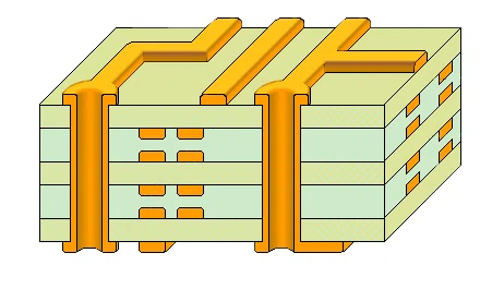
Choosing the Right Layer Stacking Structure – RF PCBs need to handle both digital signals and RF signals, which may require different grounding schemes, and therefore often require two or more dedicated grounding layers, resulting in an increase in the number of board layers. In some cases, when the digital signal frequency is high, the PCB can use mixed materials layer stack to meet the needs of different signals. The layer stack design will directly affect the alignment characteristics and the PCB manufacturing process.
Material Selection – Common FR-4 material is difficult to effectively support high frequency signals over 1 to 2 GHz and is therefore known as a standard lossy material. Although standard loss materials can still cope with higher frequency signals with shorter alignments, ideally you should refer to the material’s specification sheet, paying particular attention to its loss angle tangent or dissipation factor. A lower dissipation factor means less signal attenuation at high frequencies.
Impedance and Length Matching – Whether you are routing high-frequency signals, analogue or digital, it is important to ensure that the impedance is matched and the length of the line is matched. RF signals are typically routed with matched 50-ohm impedance alignments, and impedance consistency needs to be maintained throughout the length of the alignment. Digital signals on PCB radar is often designed with differential impedance. These digital signals typically have very short rise and fall times and transmit data through multiple channels, so length matching is necessary to ensure signal integrity.
Maintain effective grounding and shielding – To prevent crosstalk and EMI, and to improve signal integrity and electromagnetic compatibility (EMC), designs should employ a variety of grounding and shielding techniques. Maintain a continuous uninterrupted grounding layer underneath high-speed signal lines, supplemented by grounding alignments and vias to provide a complete return path for the signal.
Special attention should be paid to the fact that a grounding layer should never be installed directly underneath a PCB-mounted alignment antenna or antenna module, as this will seriously affect the antenna’s reception performance, thus reducing the overall system performance.
With the continuous development of radar technology, PCB radar as the core carrier, the complexity and importance of its design and manufacture is increasingly prominent. In the future, with the higher pursuit of radar performance in the fields of automotive radar, aerospace and defence, the PCB radar design team needs to continuously improve its professional capabilities, keep up with the latest advances in materials and processes, and promote the radar PCB technology to a higher level.