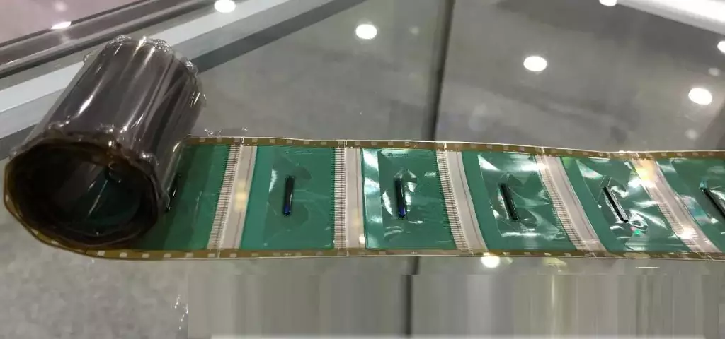
A PCB RF connector is a key component used to connect an RF circuit board to other devices, usually on a printed circuit board (PCB). Its main function is to efficiently transmit signals from inside the board to external devices, supporting the transmission of RF signals so that signals can be sent and received. The design of these connectors needs to take into account factors such as frequency range, impedance matching, and the number of plugs and unplugs to meet the needs of different applications.
RF connectors classification and name
- Coaxial RF connectors
Coaxial RF connectors are a widely used type of connector, mainly for low to medium frequency band applications. Coaxial RF connectors are divided into male and female ports,and common sizes are SMA, BNC, TNC, N, C, etc. Among them, SMA and N series connectors are the most widely used.
2.Microwave RF connectors
Microwave RF connectors are usually used for communication, radar and satellite systems applied in high frequency and microwave bands. Common models include SMP, SSMC, 2.92mm, 2.4mm and 1.85mm. Microwave RF connectors are usually made by precision crimping technology, which requires a high degree of accuracy and stability and reliability.
3.PCB RF connector
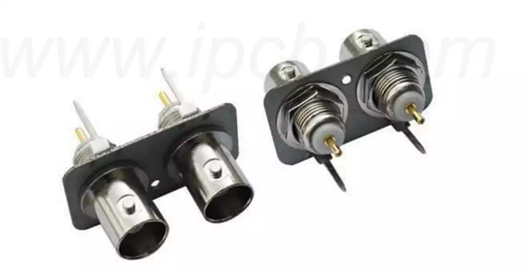
PCB RF connector is a kind of connector directly mounted on the PCB board, which can be used for lower frequency applications. Common PCB RF connectors are MMCX, MCX, SMB and SMA. Due to their small size and light weight, they are widely used in applications with weight constraints and space limitations.
- Connectors
A connector is a device that connects power or signal transmission media. Signal transmission connectors are commonly used to connect antennas, transceivers, modems and other devices. Commonly used connector types are F-type, SMA, BNC, TNC, N-type, C-type and UHF. - Adapter
Adapters are connectors used to realize the connection of different types of RF connectors, including the same type of adapters and heterogeneous adapters. The same type of adapter is the same type of two connectors through an adapter for connection, commonly used models are SMA-SMA, N-N and BNC-BNC and so on. Shaped adapters are two different types of connectors connected through an adapter, such as SMA-N adapters.
Key parameters to focus on when selecting PCB RF connectors:
- Insertion Loss
Insertion loss is the power loss incurred by the signal as it passes through the connector.This loss is usually measured in decibels (dB), lower insertion loss means higher signal transmission efficiency, so this parameter needs to be prioritized when selecting RF connectors. - Return Loss
Return loss is a measure of signal reflection ability of an indicator, reflecting the degree of signal reflection at the connector interface. The higher the return loss is, the less the reflected signal is, the better the signal integrity, thus improving the reliability and performance of the whole system. - Voltage Standing Wave Ratio (VSWR)
VSWR is an important parameter for evaluating the degree of matching between the transmission line and the load, reflecting the formation of standing waves in the transmission line. Ideally,the VSWR should be close to 1, which means that there is almost no reflection of the signal during transmission, ensuring efficient signal transmission. - Characteristic Impedance
Characteristic impedance is an important parameter set in RF circuits, which usually needs to match the characteristics of the transmission line and the system. Common characteristic impedance has 50Ω and 75Ω, choose the appropriate characteristic impedance can reduce reflection and signal distortion, to ensure good signal transmission performance.
PCB RF connector design issues needing attention
1.Layout design requirements
When designing PCB RF connector, the structural design requirements are quite important. Designers need to clarify the structure of the product to ensure that the PCB layout can effectively reflect the structural requirements, including the thickness of the outer edge of the cavity shell and the thickness of the intermediate cavity, to minimize potential interference and loss in the design process.
2.Signal path optimization
Signal path optimization is the key to achieving good electrical performance. When laying out the component locations, the RF signal path should be shortened and kept straight as much as possible to reduce signal reflection and loss, thus improving signal integrity and transmission efficiency. Excessive corners and mutations should be avoided in the layout to reduce signal attenuation and noise interference.
3.Grounding and power supply design
In RF circuits, the design of grounding and power supply is crucial for signal stability. Grounding should be as coarse as possible, and where possible, each layer of the PCB board should be laid to reduce ground impedance and provide a stable reference potential. The design of the power line is also important to avoid the formation of loops, to ensure that its direction and the RF signal parallel but not overlap, in order to reduce interference.
4.RF signal and interference source isolation
In the design process, RF signals, interference sources and sensitive signals should be effectively isolated. Through a reasonable layout and packet ground processing, you can improve the anti-interference ability of the RF signal, prevent the interference signal on the RF signal, so as to maintain the clarity and stability of the signal.
5.Consider environmental factors
Environmental factors on the design of PCB RF connectors should not be ignored. Designers need to take into account the temperature, humidity and mechanical vibration and other conditions on the performance of the circuit, and through the appropriate choice of materials and structural design to enhance the stability and durability of the circuit to ensure that the product in all types of environments can operate efficiently.
PCB RF connectors play an important role in modern electronic equipment, widely used in communications, instrumentation, navigation systems and military equipment and other fields:
Application of communication equipment
PCB RF connectors are widely used in communication equipment, mainly for wireless communication systems, cell phones and base stations. These connectors can effectively transmit microwave and radio signals to ensure the stability and reliability of the equipment working at high frequencies.
Applications in navigation systems
In navigation systems, PCB RF connectors are commonly used to connect various signal processing modules. These connectors are able to work efficiently in the frequency range of 0 to 4 GHz, ensuring accurate transmission of GPS and other navigation signals and enhancing positioning accuracy.
Instrumentation Applications
They are also indispensable components in test and measurement equipment. They connect the test instrument to the device under test, enabling the smooth transmission of high-frequency signals for accurate testing and measurement. The reliability of these connectors contributes to the credibility of the measurement data.
Medical Device Applications
In medical equipment,it is used to connect monitoring equipment to signal processing units. These connectors are capable of stable operation under high frequency conditions and provide the necessary signal support for medical monitoring. Their high reliability ensures the effectiveness and safety of the equipment in critical application scenarios.
Military Equipment Applications
In military systems, PCB RF connectors are widely used in radar and communication equipment.These equipments need to work in extremely complex and high-risk environments, and the RF connector can ensure the reliable transmission of high-frequency signals to ensure the effective operation of the system. Its excellent anti-interference ability and mechanical properties make it particularly important in the military field.
In modern electronic equipment,PCB RF connector plays an important role as the key component connecting RF circuits and external devices. They are widely used in communication, navigation, medical and military fields to provide high stability and reliability of signal transmission. With the advancement of technology and the increased demand for high-frequency signal processing, its design and optimization face new challenges and bring opportunities. In the future, through improved material and structural design, these connectors are expected to better meet the emerging industry’s demand for efficient and stable signal transmission, and drive innovation and development in related applications.