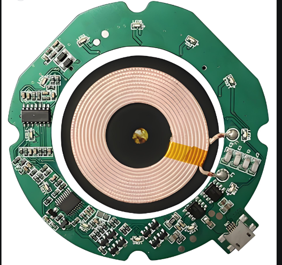
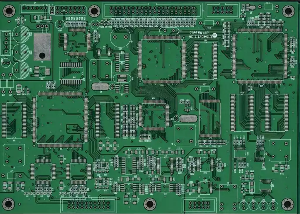
Silkscreen printing is a process of applying ink markings to a circuit board to identify the components, warning symbols, test points, markings, brand logos and other critical information on it. Generally, the component area is the preferred area for screen printing by manufacturers. Although it is sometimes found within the soldering aisle, doing so can significantly increase costs. screen printing on PCBs is an effective way for manufacturers and designers to quickly identify component layouts. It ensures accuracy when parts are reassembled. In addition, screen printing provides engineers or technicians with clear guidance on how and where components should be placed on the PCB.
The information contained in PCB silkscreen printing is rich and varied and includes:
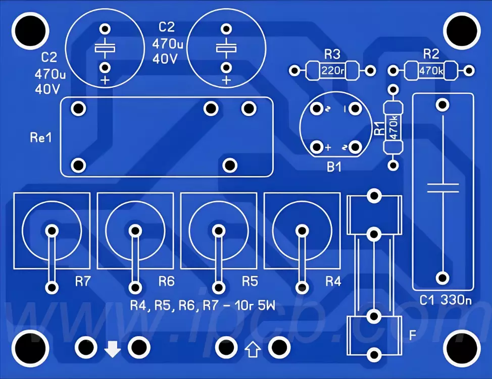
Warning symbols: These are used to highlight high temperature components that require special attention and proper care by the user during use to ensure safe operation.
Polarity markings: In order to properly mount components, polarity markings provide key information about the polarity of the component. Pin markings provide further directional guidance to ensure an accurate assembly process.
Test Point Indication: Test points are clearly labelled on the silkscreen to enable design engineers to carry out PCB testing and debugging work smoothly.
Reference Identifiers: Each assembly location has a unique reference identifier on the PCB, through which components can be accurately identified.
Numeric Codes: Unique numeric codes on the PCB silkscreen printing may represent key information such as manufacturer’s markings, version numbers, etc.
Component illustrations: For specific components such as diodes, optocouplers, etc., the component illustrations on the silkscreen ensure precise alignment during installation.
Switch Setting Instructions: Default switch setting instructions on the PCB silkscreen printing help users to better understand and use the board.
Compact Component Assistance: For compact component packages such as Ball Grid Arrays (BGAs), PIN information on the silkscreen aids in testing and debugging.
Troubleshooting and Repair Guidelines: Silkscreen markings make it easy to identify and locate individual components, which can greatly speed up troubleshooting.
Manufacturing and assembly documentation: Silkscreen markings also contain the necessary manufacturing and assembly documentation, such as copyright notices, company logos, production dates and other important information for quality control and traceability.
Branding elements: These markings not only help to enhance the aesthetics of the PCB, but also to emphasise the brand’s identity. Combining branding elements, logos and selected colours can further enhance the overall visual appeal and professionalism.
Common Silkscreen Printing Defects, their causes and solutions.
Blurred silkscreen printing: The problem may originate from insufficient screen tension, improper spacing between screen and PCB, inappropriate ink viscosity or excessive printing speed. Solutions include adjusting the screen tension to the appropriate level, optimising the spacing between the screen and the PCB, adjusting the ink viscosity and slowing down the printing speed.
Silkscreen Printing Misalignment: When the screen printing pattern does not match the pads or holes on the PCB, it may be due to insufficient positioning accuracy or mechanical vibration during the printing process. The solution is to improve the accuracy of the positioning system and reduce mechanical vibration during printing.
Uneven silkscreen printing thickness: Uneven distribution of ink on the PCB may be due to inconsistent screen aperture or uneven printing pressure. The solution is to use a screen with a uniform aperture and adjust the printing pressure to achieve even distribution.
Bubbling on the silkscreen printing surface: Bubbles appear on the ink surface after printing, which may be due to air mixed in the ink or oil on the PCB surface. Ensure that the ink is stirred sufficiently to remove air and clean the PCB surface to avoid the effect of oil.
Poor Silkscreen Printing Adhesion: Ink does not adhere well to the PCB, possibly due to improper PCB surface treatment or incompatibility between the ink and the PCB material. It should be ensured that the PCB surface is clean and properly pre-treated, as well as selecting inks that are compatible with the PCB material.
Silkscreen Printing Contamination Problems: Ink contamination to other areas of the PCB may be due to ink spillage during screen printing or unclean printing equipment. The printing equipment should be cleaned regularly and the amount of ink used should be controlled to prevent spillage.
Silkscreen Printing Colour Deviation: Printed colours do not match with expectations, which may be due to poor ink quality or improper control of colour difference during the printing process. High-quality inks should be used and chromatic aberration control should be strengthened to ensure accurate colours.
Silkscreen line breakage: Printing line breakage may be due to the ink drying too fast or printing pressure is too high. The drying speed of the ink should be adjusted and the printing pressure should be reduced to avoid line breakage.
Silkscreen printing shadow phenomenon: the printing pattern appears shadow, may be due to the screen and PCB contact is not uniform or poor ink fluidity. The contact conditions between the screen and PCB should be improved, and the ink with good fluidity should be selected to reduce the shadow.
Rough edges of silkscreen printing: Rough edges of the printed pattern may be due to improper handling of the screen edges or too fast printing speed. The screen edges should be handled properly and the printing speed should be reduced appropriately to reduce the phenomenon of rough edges.
PCB silkcreen printing provides critical information and guidance while facing multiple challenges. Through careful process optimisation and quality control, we can effectively deal with screen printing defects, ensure the high quality and reliability of PCBs, and lay a solid foundation for electronic product manufacturing.