Definition and Importance of PCB Sockets
In modern electronics manufacturing, with the increasing complexity and modularity of equipment functions, the flexibility and reliability of circuit connections have become key design factors. PCB sockets play a crucial role in this context. They are not only a bridge connecting components to the motherboard, but also a vital infrastructure supporting stable operation, convenient maintenance, and modular upgrades of electronic systems.
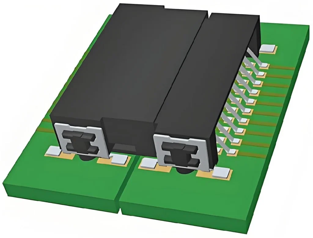
A PCB socket is a pluggable connector mounted on a printed circuit board to transmit electrical signals, power, or data. It typically consists of conductive metal terminals and an insulating plastic housing, allowing for mechanical and electrical connections with corresponding plugs or pins. Unlike traditional soldering connections, PCB sockets allow components to be easily installed, replaced, or tested without damaging the circuitry, greatly improving the maintainability and flexibility of electronic systems.
PCB sockets are ubiquitous in complex electronic devices such as communication equipment, servers, automotive electronics, industrial control systems, and wearable devices. They serve the dual purpose of signal transmission and electrical interface within the system. On the one hand, it ensures low-loss transmission of high-speed signals between different modules; on the other hand, it provides physical support and reliable contact for pluggable components (such as CPUs, sensor modules, and RF modules). In other words, the quality and design of PCB sockets directly affect the performance stability and lifespan of the entire system.
From a manufacturing and application perspective, the importance of PCB sockets lies not only in their connectivity but also in the system optimization and cost-effectiveness they bring. For product designers, using a socket structure enables “plug-and-play” modular design, facilitating subsequent functional expansion and upgrades. For example, during the testing phase, engineers can quickly replace chips or modules using sockets without repeating soldering operations, significantly saving development time and reducing prototype debugging costs. In large-scale production and maintenance, the use of sockets makes product repair, upgrades, and testing more efficient, reducing production losses caused by soldering rework.
The strategic significance of PCB sockets also lies in their support for the reconfigurability and sustainable development of electronic systems. In the past era of electronics manufacturing, once circuits were soldered, module replacement or technological updates were virtually impossible. Today, however, thanks to socket structures, designers can replace core components without altering the overall device structure, thereby extending the device’s lifespan and reducing electronic waste. This is especially important in today’s context of advocating green manufacturing and a circular economy.
At a deeper level, the development of PCB sockets also reflects the evolution of the electronics manufacturing industry towards high-density integration and intelligence. With the continuous advancement of chip packaging technologies (such as BGA, QFN, and LGA), the requirements for the precision and stability of connection interfaces are becoming increasingly stringent. Traditional soldering methods are prone to micro-cracks or poor contact under repeated insertion/removal, thermal cycling, and vibration conditions. High-performance PCB sockets, through flexible contacts, gold plating, precision molding, and shockproof design, effectively solve these reliability issues, making them an indispensable component of high-end electronic systems.
In today’s world where electronic products are constantly pursuing miniaturization, high speed, and maintainability, PCB sockets are not merely connectors, but also an embodiment of an engineering philosophy—giving complex systems replaceable, upgradeable, and verifiable capabilities. It can be said that any modern electronic design that requires a balance of performance, flexibility, and maintainability cannot function without this fundamental yet crucial component.
PCB Socket Structure and Classification
To deeply understand the technical value of PCB sockets, it is essential to begin with their structural composition and classification. Although different types of sockets differ in form, application, and manufacturing process, their core objective remains consistent—to provide stable and repeatable electrical and mechanical connections within a limited space.
Structurally, a standard PCB socket typically consists of the following key components: contact terminals, insulator, mounting structure, housing, and in some high-end models, a shielding layer and locking mechanism.
Contact terminals are the core component for signal transmission, typically made of highly conductive copper alloys or phosphor bronze, and plated with gold or nickel to improve corrosion resistance and conductivity. Terminal shapes can be categorized into pin-shaped, spring-loaded, or blade-shaped structures depending on their application. Spring-loaded terminals automatically compensate for minor mechanical deviations during repeated insertion and removal, maintaining stable contact pressure and preventing signal loss.
Insulators are responsible for maintaining electrical isolation and support between terminals. They are typically made of high-strength engineering plastics such as PBT, LCP, or PA66 to ensure no deformation or dielectric breakdown occurs under high-temperature soldering or prolonged operation.
In terms of mounting structure, PCB sockets can be divided into through-hole type (Through-Hole) and surface mount type (SMT). Through-hole type sockets allow leads to pass through PCB holes and are wave soldered or hand-soldered, providing strong mechanical stability and suitable for applications requiring high vibration resistance or frequent insertion and removal. SMT type sockets are directly soldered to the PCB surface and are suitable for high-density assembly and automated production. In recent years, with the increasing demand for high-frequency signals and high-speed transmission, more and more high-end sockets adopt SMT structures, combined with embedded shielding or grounding designs, to reduce parasitic effects and signal interference.
Based on application and interface characteristics, PCB sockets are classified in great detail, but can be broadly categorized as follows:
IC Sockets
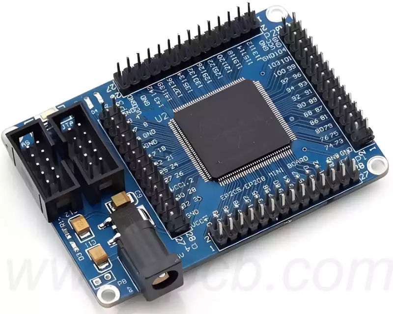
This is the most common type, primarily used for mounting integrated circuit chips, such as DIP, SOP, QFP, BGA, and LGA packages. IC sockets enable electrical connections without soldering the chip, facilitating testing, maintenance, and upgrades. Especially in bottom-ball packages like BGA and LGA, sockets avoid damage caused by high-temperature soldering, improving replaceability.
Pin Header Sockets
These sockets connect to pin headers and are commonly used in modular designs, signal output, or power distribution. They typically have dual or multi-row sockets, compatible with different pitch specifications (e.g., 2.54mm, 1.27mm), and are widely used in development boards, control modules, and communication equipment.
RF/Coaxial Sockets
Designed specifically for radio frequency signals, these provide low-reflection, low-loss connections at GHz and even millimeter-wave frequencies. Typical structures include interfaces such as SMA, SMB, MCX, and MMCX, commonly used in RF modules, antenna connections, and test platforms. High-frequency PCB materials from Rogers and other manufacturers are often used with these sockets to ensure signal integrity.
Modular/Custom Sockets: Designed for specific equipment or industrial applications, these sockets may integrate power/signal mixed contacts, shielded enclosures, and snap-fit mechanisms. They offer high flexibility and are typically used with specific brands or systems in automotive electronics, medical instruments, and server motherboards.
Test/Burn-in Sockets: These sockets are primarily used for functional verification and lifespan testing of chips or modules. They require extremely high insertion/removal lifespan and signal accuracy, therefore typically employing highly elastic alloy materials and precision machining processes to support tens of thousands of insertion/removal cycles. They are commonly found in semiconductor test equipment, ATE systems, and R&D laboratories.
In addition to the above categories, there are some subcategories, such as battery sockets, sensor sockets, memory sockets (DIMM sockets), and CPU sockets. These sockets differ not only in size and shape but are also specifically optimized for parameters such as current carrying capacity, signal rate, insertion/removal cycles, and mechanical strength.
It is worth noting that as electronic devices trend towards miniaturization and higher frequencies, the structural design of sockets is becoming increasingly complex. Modern PCB sockets are no longer merely passive connection components but highly engineered system components. They need to achieve precise matching within micrometer-level tolerances while balancing mechanical stress, electromagnetic interference, and thermal management. Especially in CPU or GPU-level sockets, hundreds or even thousands of contacts must simultaneously maintain precise alignment and uniform contact pressure, placing extremely high demands on manufacturing processes.
It can be said that the structural design of PCB sockets is both the core of connection technology and a hallmark of manufacturing prowess. It must ensure contact reliability while adapting to multiple challenges such as automated assembly, high-speed signal transmission, and thermal cycling. From microscopic contacts to the overall package, every detail directly affects the performance and lifespan of the electronic system.
PCB Socket Materials and Manufacturing Processes
While PCB sockets may appear simple in appearance, their internal structure and material selection reflect extremely high engineering complexity. A high-quality socket must simultaneously meet multiple requirements, including conductivity, mechanical strength, high-temperature resistance, corrosion resistance, signal integrity, and long-term stability. Achieving these performance characteristics relies heavily on strict control over materials and manufacturing processes.
At the materials level, the main components of a PCB socket include metal contact terminals and an insulating support structure. The metal portion is the core for signal and power transmission, and its conductivity directly determines the transmission efficiency and stability of the entire system. Common metal materials include phosphor bronze, beryllium copper, brass, and nickel-chromium alloys (Ni-Cr alloys) used in some high-end models.
Beryllium copper is widely used in high-frequency sockets due to its high elasticity and excellent conductivity. It maintains good elastic recovery after repeated insertions and removals, preventing contact loosening. Phosphor bronze is widely used in general-purpose sockets due to its cost advantage and good mechanical strength. For industrial or aerospace products requiring high-temperature resistance and corrosion resistance, nickel alloys or multi-layered composite metal structures are used to ensure reliable contact performance in extreme environments.
The plating process on the metal surface is a crucial step in ensuring the long-term performance of a socket. Commonly used plating materials include gold (Au), nickel (Ni), tin (Sn), and silver (Ag). Gold plating is most common in high-end sockets because gold has excellent oxidation resistance and low contact resistance, significantly improving signal transmission stability and insertion/removal life. Nickel plating is often used for bottom layer protection, effectively preventing gold layer diffusion or corrosion. Some mid-to-low-end products use tin plating to reduce costs, but it is prone to oxidation after repeated insertions and removals, and is therefore generally used in applications with lower lifespan requirements. To further improve contact reliability, some manufacturers also use a “zoned plating” process, applying a thick gold plating to the contact area and a nickel plating to the soldering area to balance performance and cost.
The choice of materials for the insulator is equally important. It must not only provide mechanical support but also maintain electrical isolation between contacts. The most commonly used insulating materials include PBT (polybutylene terephthalate), LCP (liquid crystal polymer), PA66 (nylon 66), and PPS (polyphenylene sulfide). LCP (Lithium Chromium Plating) is widely used in high-density and high-frequency sockets due to its high heat resistance, low moisture absorption, and excellent dimensional stability. LCP has an extremely low coefficient of thermal expansion after molding, ensuring precise contact positioning even during repeated thermal cycling. PBT (Polymer Bitrate) and PA66 (Polyester Aluminum Butylene) offer better toughness and formability, making them suitable for socket structures in general consumer electronics. For applications in extreme environments (such as automotive engine compartments and aerospace systems), PPS (Polyester Polymer Stainless Steel) is the preferred choice due to its excellent chemical resistance and high-temperature stability.
In terms of manufacturing processes, PCB socket production typically includes stamping, plating, injection molding, automated assembly, and testing.
Stamping: Contact terminals are usually processed using high-precision stamping dies. This process requires strict control of die clearance and stamping pressure to ensure precise consistency in the terminal’s geometry and elasticity curve. Any minute error can lead to poor insertion/removal contact or signal reflection.
Plating: The stamped metal terminals undergo electroplating, with appropriate plating thickness and materials selected based on different functional areas. The gold layer thickness of high-end products is generally controlled between 0.76μm and 1.27μm to ensure long-term wear resistance and low contact resistance.
Injection Molding: The insulator is manufactured using injection molding. The precision of the mold directly determines the insertion and removal alignment accuracy of the socket. In recent years, with the popularization of micro-pitch design, some manufacturers have adopted precision multi-cavity molds and LCP micro-injection molding technology to achieve socket structures with a pitch of less than 0.4mm.
Automatic Assembly & Inspection: During the assembly stage, the terminals and insulators require precise positioning and mechanical pressing. High-end production lines have introduced automated vision inspection systems that can monitor parameters such as terminal angle, insertion force, and alignment in real time to ensure that each socket meets the standard requirements. Some sockets also undergo “insertion and removal life tests” and “high-temperature aging tests” before leaving the factory to verify their durability and stability.
It is worth mentioning that with the development of high-speed signal and high-frequency communication technologies, many innovative processes have been introduced into socket manufacturing. For example, technologies such as precision micro-spring structures to achieve adaptive contact pressure, laser welding and metal injection molding (MIM) to improve structural precision, and shielding coatings to reduce electromagnetic interference enable sockets to operate stably at higher frequencies and in more demanding environments, particularly excelling in 5G, millimeter-wave radar, and server-grade applications.
In short, every minute structural and technological aspect of a PCB socket embodies engineering ingenuity. From materials to manufacturing, from structure to process, it not only reflects the precision of electronic connectivity technology but also the manufacturer’s accumulated expertise in reliability and performance optimization. Therefore, the development and manufacturing of high-quality sockets often becomes a key differentiator between high-end and ordinary electronic products.
PCB Socket Manufacturing Process and Quality Control
In modern electronics manufacturing, the manufacturing process of a PCB socket directly determines the reliability, electrical performance, and lifespan of the connection. Although it may seem like a small interface component, every step, from material selection and electroplating thickness control to injection molding precision and plating uniformity, involves the accumulation of high-precision manufacturing technologies. To understand the creation of a high-quality socket, one must delve into the details of its manufacturing process and the logic of quality management.
First, there is material selection. High-quality PCB sockets typically use high-temperature resistant plastic substrates, such as LCP (liquid crystal polymer), PBT, PA9T, or PEEK. These engineering plastics possess excellent dimensional stability and low moisture absorption, maintaining their shape and strength even in the high-temperature environments of wave soldering or reflow soldering. Metal components often use phosphor bronze, beryllium copper, or stainless steel, with phosphor bronze being the most common due to its excellent elasticity and high conductivity. Different metal materials are also paired with different plating processes, such as gold plating, tin plating, and nickel plating, to improve the corrosion resistance and conductivity of the contact surface.
Next comes the stamping and forming process. Metal terminals are typically stamped at high speed in molds using precision stamping presses. The design of the stamping die directly affects the springiness, flatness, and dimensional consistency of the pins. For high-density signal transmission sockets, the terminal shape is more complex, sometimes requiring multiple processes to complete the internal and external bending and positioning groove forming. The plastic shell is made using injection molding, which requires the filling and cooling of molten plastic to be completed in a very short time. The mold precision is usually controlled within ±0.01mm; otherwise, the socket fit may be too tight or too loose, affecting the overall assembly performance.
In the electroplating process, the precision of the surface treatment directly determines the electrical performance and durability of the socket. Gold plating effectively reduces contact resistance while preventing oxidation and sulfidation. Generally, signal sockets use a gold plating process with a thickness of 3–50 μin, while power sockets focus more on the wear resistance and conductivity balance of the nickel plating layer. Advanced manufacturers also use selective electroplating technology, plating gold only in specific contact areas to reduce costs while maintaining performance stability.
Assembly processes present another test of precision. Every component on an automated assembly line must be inserted or soldered into the PCB with high consistency. For detachable sockets, the balance between insertion/extraction force and holding force must be controlled. Excessive insertion/extraction force leads to accelerated pin wear; insufficient force easily causes poor contact. Modern factories use automated testing systems to monitor these physical characteristics in real time, ensuring each socket is within the ideal parameter range.
Quality control is integrated throughout the entire manufacturing process. In addition to routine dimensional inspections and visual checks, a series of electrical and mechanical performance tests are conducted. These include insertion/extraction life tests (typically requiring over 500 cycles without failure), contact resistance tests (generally requiring less than 20mΩ), and soldering temperature tests (up to 260°C without deformation). For sockets used in high-frequency applications, impedance matching and signal loss characteristics are also tested to ensure stable performance even under GHz-level signal transmission.
With the advancement of smart manufacturing, more and more PCB socket manufacturers are introducing automated optical inspection (AOI), coordinate measuring machine (CMM), and X-ray solder joint analysis to achieve end-to-end traceability management from production to shipment. Advanced companies have even established digital twin systems to model process parameters such as temperature, pressure, and time during socket manufacturing in real time, enabling them to predict potential defects and optimize accordingly.
In summary, PCB socket manufacturing is not merely a mechanical assembly process, but a fusion of materials science, precision engineering, and electronic technology. Every inch of its metallic sheen and every contact point’s elasticity reflects an extreme pursuit of reliability and stability. A small socket often embodies the combined effect of hundreds of process details and quality standards. It is these rigorous manufacturing and testing processes that allow sockets to play a stable and crucial role in complex circuits, becoming the silent yet irreplaceable “connection heart” of electronic systems.
Future Trends and Innovation Directions of PCB Sockets
As electronic devices evolve towards higher speeds, miniaturization, and intelligence, the technological evolution of PCB sockets has entered a new stage. Future socket development will not only focus on extending lifespan or increasing insertion/removal cycles, but also on multi-dimensional performance indicators such as signal integrity, thermal management, automated assembly compatibility, and sustainable manufacturing.
Firstly, in high-frequency and high-speed applications, traditional pin-type connections are no longer sufficient to meet the demands of several GHz or even millimeter-wave signal transmission. To reduce reflections, signal crosstalk, and attenuation, high-end sockets are incorporating precision micro-spring structures, low-dielectric-constant materials, and partial shielding designs. By optimizing terminal shape, contact pressure, and arrangement density, sockets can achieve high-fidelity transmission of high-speed signals while maintaining ease of insertion and removal, which is particularly crucial for 5G communications, radar systems, satellite communications, and high-speed computing platforms.
Secondly, as electronic products move towards miniaturization and high-density integration, socket sizes are continuously shrinking while the number of contacts is increasing. This demands higher precision in materials and manufacturing processes. The use of liquid crystal polymers (LCPs), high-performance nylon, and composite materials allows sockets to maintain good mechanical strength and insertion/removal life even in micro-pitch environments. Furthermore, the introduction of 3D printing and micro-precision machining technologies provides a feasible path for customized sockets, especially suitable for specialized fields such as medical, aerospace, and scientific research experiments.
Thirdly, thermal management and environmental adaptability are becoming important directions for future socket design. With increasing chip power consumption, high-density modules may generate significant heat, and traditional sockets may deform or experience poor contact under prolonged high temperatures. Therefore, new sockets are employing high-temperature resistant materials, thermally conductive plastics, and metal heat dissipation structures to maintain reliable contact during continuous operation or in extreme environments, while also ensuring system heat dissipation performance.
Fourth, automation and testability are also driving socket technology innovation. Modern production lines require sockets to interface with PCBs quickly and efficiently, while also supporting in-circuit testing and functional verification. To this end, manufacturers have designed plug-in structures adaptable to robotic operation, automatic positioning latches, and quick-release modules, making the entire production and maintenance process more intelligent. Some high-end sockets also integrate miniature testing interfaces, enabling real-time monitoring of connection status or temperature and current data, providing a fundamental guarantee for smart factories and IoT devices.
Fifth, environmental protection and sustainable manufacturing are increasingly becoming design considerations. Future socket material selection and manufacturing processes will place greater emphasis on recycling and low carbon emissions. For example, reducing gold plating, using recyclable plastics, optimizing production energy consumption, and extending product lifespan not only reduce environmental burden but also align with global trends in green manufacturing and sustainable development.
Furthermore, modularity and upgradeability will continue to strengthen the strategic value of sockets. In smart home appliances, servers, industrial control, and automotive electronics, detachable and upgradeable socket designs enable modular updates without requiring a complete system replacement. This not only reduces operating costs but also enhances device flexibility and user experience.
Finally, with the rise of emerging technologies such as artificial intelligence, the Internet of Things, and quantum computing, the application of PCB sockets in cutting-edge fields such as high-performance computing and microwave quantum devices will further expand. This demands unprecedented levels of socket performance in terms of micron-level tolerances, high-speed signal integrity, heat and corrosion resistance, and multifunctional integration.
In conclusion, future PCB sockets will not merely be physical interfaces for connecting devices, but rather comprehensive technological systems integrating high-speed transmission, heat resistance and reliability, intelligent manufacturing, sustainability, and modular upgrades. They will continue to play a core role in electronics manufacturing, communications, industrial control, and cutting-edge scientific research, providing solid support for the stable, efficient, and sustainable development of electronic systems.
Summary
Although PCB sockets are tiny in size within electronic systems, they carry extremely important functional value. They are not only key interfaces for achieving modular design and rapid replacement but also fundamental components for ensuring signal integrity, system reliability, and long-term stable operation. Through precise material selection, advanced manufacturing processes, and rigorous quality control, modern sockets maintain excellent performance even in high-speed, high-frequency, and high-density electronic environments. Meanwhile, as electronic products evolve towards intelligence, miniaturization, and green sustainability, socket technology continues to innovate, evolving towards high performance, upgradeability, environmental resistance, and compatibility with automated production. It can be said that PCB sockets are not merely physical interfaces for connecting devices, but also core elements supporting the efficient operation and sustainable development of modern electronic systems.