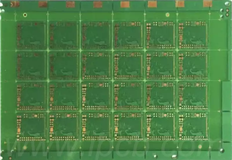
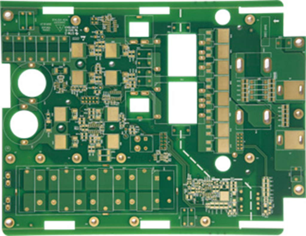
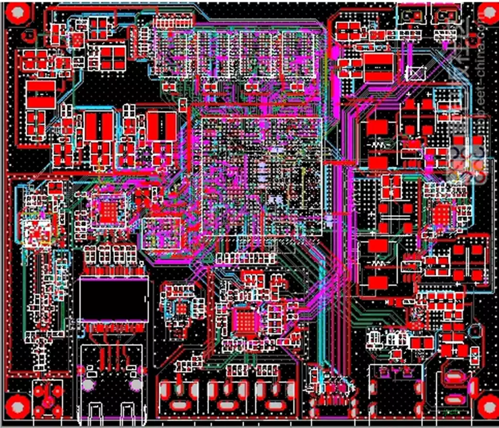
Solder mask is a key technology in the manufacture of PCBs (Printed Circuit Boards), designed to protect the metal components of the board from oxidation and to avoid the formation of conductive bridges between the pads. Soldermask is particularly important in processes such as reflow or wave soldering, where it is difficult to precisely control where the molten solder lands on the board, which can be achieved to some extent with soldermask. The soldermask is sometimes referred to as ‘solder resist’, a more appropriate term as it is often mistakenly thought that the soldermask is the solder that covers the entire layer of the circuit board.
Types of PCB solder Resist
Solder mask consists of a polymer layer applied to the metal traces of a printed circuit board.There are many different types of PCB solder resist,and the choice of which type to use depends largely on cost and application requirements.The most basic method of soldermask is to screen print a liquid epoxy resin,similar to the process of spraying paint through a stencil,in a variety of colours.
Liquid Epoxy solder mask
Applying liquid epoxy to PCBs using screen printing techniques is the most basic and cost-effective soldermask option. The process uses a woven mesh to support the ink resist pattern. Liquid epoxy is a thermosetting polymer that cures and hardens when heated. The desired colour of the resist is achieved by mixing the resist dye into the liquid epoxy.
Liquid Photoimageable solder mask (LPSM)
More advanced solder mask technology utilises a photolithographic process of dry film or liquid soldermask, similar to the photoresist exposure process used in semiconductor manufacturing.LPSM can be applied either by screen printing or by spraying, with the latter usually being more economical. A more advanced (and accurate) method is to use photolithography to define soldermask openings for pads, vias and mounting holes. A photolithography mask matching the desired soldermask is created from a Gerber file, and the board is then thoroughly cleaned to ensure no dust remains. Afterwards, liquid LPSM is applied to fully cover both sides of the board.
In LPSM applications, the black portion of the photolithography mask indicates the areas where conductors are expected to be exposed, while the areas of the board expected to be covered with soldermask remain transparent. After applying the LPSM, the board is dried in an oven and placed in a UV developer. A photolithographic mask is precisely aligned on the dried board and the board is subsequently irradiated with UV light. exposed areas of the LPSM material are cured by the UV light, while the unexposed areas are removed with a solvent, leaving a hard soldermask.
Dry Film Solder mask (DFSM)
DFSM solder mask uses a similar process to LPSM. Both PCB solder mask types are exposed during the lithography process. Unlike liquid coatings, dry film soldermasks are applied in the form of soldermask sheets using vacuum lamination. This vacuum lamination step ensures that the unexposed soldermask fits tightly to the board and removes air bubbles from the film. After exposure, the unexposed areas of the soldermask are removed with a solvent and the remaining film is cured in a heat treatment process.
Top and Bottom Solder mask
In other guides to PCB solder mask types, top and bottom soldermasks are often mentioned. These two types refer only to specific soldermasks located on the top or bottom of the board and do not involve a specific manufacturing process or a specific type of soldermask material.
Final Steps: Curing and Surface Preparation
After the application of the above media, the board is cleaned to remove all dust. The board then undergoes a final hardening and curing process. The liquid epoxy soldermask is cured thermally without UV exposure, while the LPSM and DFSM films are cured by UV exposure during the lithography process. After exposure, these films are further cured and hardened by heat treatment.
Regardless of the type of PCB solder resist used,the resulting soldermask will leave bare copper areas on the board.These exposed areas must be coated with a surface treatment to prevent oxidation.The most common surface treatment is hot air solder levelling (HASL),although other popular treatments include electroless nickel immersion gold (ENIG) and electroless nickel chemical palladium immersion gold (ENEPIG).If applicable,additional holes are reserved in the diaphragm layer for the flux layer. Flux layers are used to attach pads or other components to the printed circuit board and are treated differently depending on the manufacturing process.
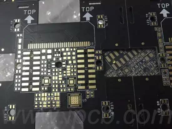
When choosing the right solder mask,you need to consider the physical specifications of the board, holes, components and conductors, the surface layout, as well as the final application scenario of the product.First and foremost,if your PCB solder resist will be used in a ‘high reliability’ application such as aerospace, telecoms, medical, etc., be sure to review the relevant industry standards for soldermasks as well as your specific application expectations as these specific requirements may go beyond the generic recommendations available on the web. For most modern PCB designs,photolithographic soldermasks are an essential choice, and the characteristics of the surface pattern will determine whether liquid or dry application is used.
Dry application creates a uniform thickness of solder resist over the entire surface, but the best adhesion is usually found when the board surface is extremely flat. If the surface features are complex and variable, liquid soldermask (LPSM) may be a better choice because it provides better contact with copper traces and laminates. However, the disadvantage of liquid application is the difficulty of ensuring a perfectly uniform thickness across the board. In addition, there are variations in the results of treatments on the laminate layers, so it is critical to communicate with the manufacturer about the types of products they offer and their impact on production. For example, when using a solder layer reflow process, a matte finish can help reduce the formation of solder balls. For PCBs manufactured through the solder reflow process, the finish of the solder resist layer will have a direct impact on the quality of the reflow.
When designing a PCB layout, the solder resist layer should be represented as separate layers (top and bottom) in your Gerber file and PCB layout.This is not defined in the Layer Stacking Manager, but is usually preset as an additional layer in the CAD tool. If the soldermask is not fully centred, it is usually necessary to leave 2 mils of border space around the component. Also, the minimum distance between pads is usually set at 8 mils to ensure that the diaphragm is effective in preventing the formation of solder bridges.
Choosing the right solder mask is critical to the reliability and performance of the PCB. Designers need to consider the board specifications, layout, application scenarios and costs to make a wise choice of solder mask types such as liquid epoxy, LPSM or DFSM. At the same time, ensure that the solder resist is presented as a separate layer in the layout design and follow industry standards to optimise PCB quality and productivity.
