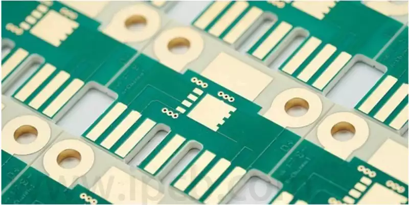
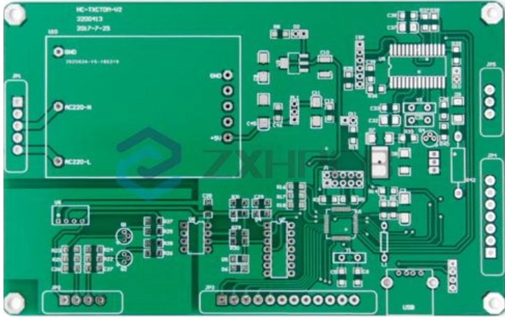
Soldermask, as a thin layer of polymer, serves the primary purpose of protecting the copper layer on a circuit board from the risk of oxidation and short circuiting during manufacture and use. At the same time, it provides the PCB with an additional layer of environmental barrier. The thickness of the soldermask is usually closely related to the thickness of the copper traces on the board and varies in different locations such as the LPSM and DPSM areas. Typical soldermask thickness is at least 0.8 mils, and may drop to 0.3 mils or less near the wire edges. A minimum of 0.5 mils of soldermask over the trace is usually required to ensure a quality weld. A sprayed epoxy soldermask helps to achieve uniformity of thickness across the PCB.
Types of PCB Soldermask
Top and Bottom Soldermask: Engineers often use these two types of soldermask to mark openings in the green soldermask on a circuit board, which is added by epoxy or film methods. Component pins are then soldered to the board through the registered openings. The alignment at the top of the board is called the top alignment and its corresponding soldermask is the top mask, the same for the bottom.
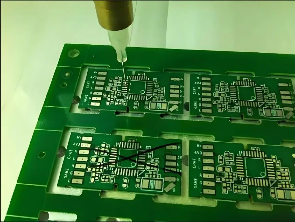
Liquid Epoxy Soldermask: As a cost-effective alternative to soldermasks, epoxy is applied to PCBs through screen printing techniques. Screen printing uses a woven mesh to support the ink resist pattern, identifying open areas through the mesh for ink transfer, followed by a heat curing process.
Liquid Photo Imaging (LPI) Solder Resists: LPI solder resists are made from a blend of two different liquids that are stored separately prior to application to extend shelf life.LPI is suitable for a variety of applications including curtain coating, screen printing, and spray coating. It is characterized by its sensitivity to UV light and requires exposure to UV light after a short “tack-cure cycle”.
Application of LPI Soldermask: Prior to application, the panel is cleaned and inspected for signs of oxidation. This is accomplished by scrubbing the panel with a chemical solution, aluminum oxide solution or suspended pumice. Subsequently, the panels are processed by UV exposure using thin film tools and contact printers, or by direct laser imaging.LPI masks are available in a wide range of color options, such as green, black, red, etc.
Dry Film Photoimageable Solder Resist: This type of solder resist is fabricated through the steps of vacuum lamination, exposure and development. High-density PCBs are particularly suitable for dry film soldermasks because they do not flood the vias.
Surface Preparation: Different types of PCB board soldermasks require surface preparation of the exposed copper areas to prevent oxidation. Hot Air Solder Leveling (HASL) is one of the popular treatments, but other methods such as Electroless Nickel Palladium Immersion Gold (ENEPIC) and Electroless Nickel Immersion Gold (ENIG) are also available upon request.
How to choose the right soldermask?
Choosing the right soldermask depends on the physical dimensions of the board, holes, components and conductors, the surface layout and the final application of the product. First and foremost, industry standards and application requirements should be considered, especially in high-reliability industries. For most modern printed circuit board designs, photolithographic soldermasks are preferred. The surface pattern will determine whether a liquid or dry application is used. Dry application creates a uniform thickness of soldermask over the entire surface, but if the surface features are complex, the liquid (LPSM) option may be more suitable. It is also important to discuss with the manufacturer how different finishes will affect production.
Solder Resist Thickness Selection
In general, soldermask thickness depends on the type of board being used and the level of protection required. Excessively thick soldermask can cause connection problems, so it is important to choose the thickness of the soldermask appropriately.
For regular circuit boards, the thickness of the soldermask can be selected between 0.02mm and 0.05mm. However, in high-density circuit boards, a thinner soldermask may be a better choice because it can better protect small electronic components. And in high power circuit boards, thicker soldermasks can better protect board components.
In PCB manufacturing, choosing the right soldermask Thickness is critical to ensuring product Quality and Reliability. From liquid epoxy soldermasks to dry film photoimageable soldermasks, each type has its own unique applications and benefits. Therefore, an in-depth understanding of the characteristics, performance and scope of application of each type of soldermask, as well as making an informed choice based on actual needs, is critical to improving the overall performance and extending the service life of the PCB.
