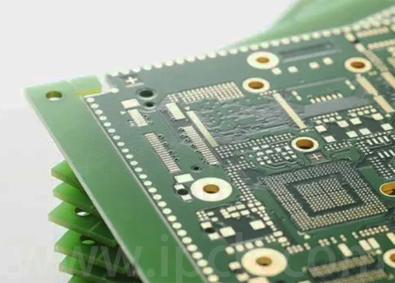
PCB thickness tolerance refers to the difference in the thickness of a circuit board due to the production process and equipment conditions during the manufacture of the pcb circuit board, which is the thickness tolerance of the board. This tolerance range depends mainly on the type and specification of the board used.
Normally, the pcb thickness tolerance standard for circuit boards follows the principle of ±10%. This means that if the nominal thickness of a circuit board is 1.6mm, then in actual production, its thickness can fluctuate between 1.44mm and 1.76mm. Such a tolerance range is intended to accommodate the various factors that may occur during production, such as variations in materials, processes and the environment, thus ensuring the stability and reliability of the circuit board.
In addition to the general principle of ±10%, pcb thickness tolerance varies depending on the specific pcb thickness. The following are some common board thicknesses and their corresponding tolerance ranges:
- For 0.5mm pcb thickness, the coarse tolerance is ±0.07mm, the fine tolerance is ±0.01mm.
- For 1.0mm pcb thickness, the coarse tolerance is ±0.17mm and the fine tolerance is ±0.11mm.
- For thicker 2.0mm boards, the coarse tolerance is increased to ±0.23mm and the fine tolerance is ±0.15mm.
These specific tolerances help manufacturers to more accurately control the quality of circuit boards and meet the needs of different application scenarios.
IPC (Institute of Printed Circuits) is the international association of printed circuits. ipc has established a number of industry standards, including PCB manufacturing standards and inspection standards. One of the necessary IPC standards specifies the proper thickness of PCB boards.
According to IPC-A-600, the range of PCB thickness tolerance is the percentage of the board thickness and its tolerance.The IPC-A-600 standard specifies the thickness tolerance of PCB board as follows:
Base material min. 0.07 mm, tolerance:
Single panel ± 0.03 mm;
Double-sided board ± 0.06 mm;
Multi-layer board ± 0.10 mm;
Copper thickness min. 18um, tolerance:
Single panel ±0.025mm;
Double-sided board ±0.05mm;
Multilayer board ± 0.075mm;
Therefore, according to the IPC standard, PCB thickness tolerance should be calculated based on the minimum value of its base material and the minimum value of copper thickness to achieve the proper tolerance range to ensure that the board will work correctly.
Methods for adjusting pcb thickness tolerance
1.Material Adjustment:
- Selection of substrates with more stable thickness can reduce pcb thickness tolerance.
- Selection of copper cladding foils with smaller thickness tolerances can adjust the thickness of the copper cladding foils to better control the pcb thickness tolerance.
2.Technological adjustment:
- Selecting a finer cladding method can effectively reduce the pcb thickness tolerance range.
- Adopting more delicate pressure-sensitive film process can improve the pcb thickness accuracy.
3.Manufacturing equipment adjustment:
- Selection of high-precision manufacturing equipment can effectively improve the manufacturing accuracy, thereby reducing the pcb thickness tolerance range.
- Formulate a reasonable process to avoid human error, to ensure that the pcb thickness tolerance is more accurate.
What are the factors affecting the selection of PCB thickness?
1) Copper Thickness
Copper thickness depends on the amount of current the PCB needs to carry, and will be adjusted according to the specific requirements of the board. At the same time, copper thickness also affects the cost, the thicker the board, the higher the cost due to increased material requirements and processing difficulties.
2) Substrate
Substrates and laminates are the basis of PCB. The substrate is a non-conductive dielectric material with a dielectric composite structure, and its selection is usually based on the dielectric constant. Common substrates consist of epoxy resins and paper, sometimes enhanced with ceramics to allow manufacturers to meet performance requirements such as glass transition temperature (i.e. the point at which heat causes the material to soften and deform).
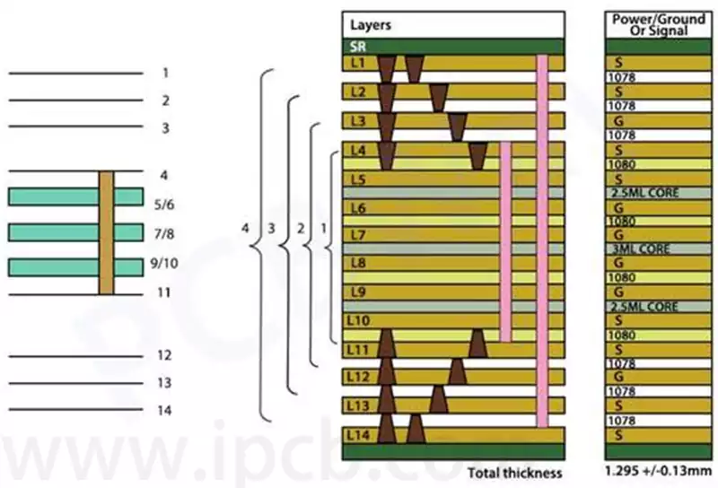
3) Number of PCB Layers
It is well known that the number of layers in a PCB affects its thickness. 2-6 layer PCBs may be of standard thickness, while 8 layer and above PCBs may be out of the standard thickness range. If the PCB requires more layers, do not try to achieve the standard thickness with thinner layers, as this may be impractical.
4) Signal Types
PCBs use a variety of signal types to determine the materials required, which in turn affects their thickness. For example, PCBs carrying high power signals need to be thicker and have wider copper alignments, and the need for high power alignments will make the PCB thicker.
5) Type of Through Hole
In order to create a compact PCB design, through-hole routing needs to be routed through the board and not on its surface. There are different types of via holes such as through holes, microvias, blind holes, buried holes, and solder pad internal holes. The density and type of vias play an important role in determining the thickness of the board.
6) Use of the environment
The conductivity and resistance of a circuit board depends on the thickness of the PCB and the materials used in its manufacture. Thin PCBs may not be suitable for harsh operating environments. PCBs with thick copper traces are less thermally stable under high currents. In addition, the connectors and components of the PCB are also related to the thickness of the board due to specific material and performance requirements.
Effective control of pcb thickness tolerance is key to product quality. By optimising materials and processes, the stability and performance of circuit boards can be improved to meet the needs of diverse applications.