The pcb trace width calculator is a device that relies on the IPC 2221 formula to determine the width of PCB alignments and is specifically designed to help designers determine the optimal width of alignments on PCBs (Printed Circuit Boards) to ensure the safety and reliability of circuits.
The trace width is a key factor to consider when designing a printed circuit board. In fact, you must assign the correct width to the alignments to prevent them from being damaged by high temperatures. It is best to design the alignment on the PCB so that it can withstand the maximum current load before failure occurs. Remember, as you conduct more current through a path, it will start to heat up. Therefore, when the current load exceeds the upper limit, the alignment can burn or damage the circuit board’s laminate. This can lead to permanent PCB damage. You can compare PCB alignments to the wires connecting various zero-resistance components. However, each PCB path contains its own resistance, which is an essential factor when choosing the width of the PCB trace.
Therefore, you need to know the resistance and current carrying capacity to define the width that will be used. It is important to note that temperature rise can affect the width of the trace. Temperature rise is the temperature of the trace when the current is on and off. In other words, simply subtract the operating temperature from the higher operating temperature to obtain the temperature rise.
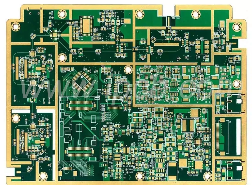
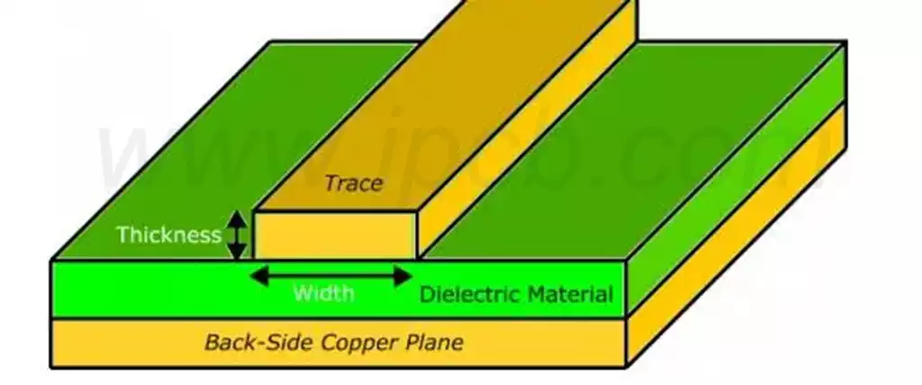
PCB traces are thin conductive copper wires placed on a non-conductive or isolated substrate to carry signals and power throughout the circuit. Copper traces have a specific width, which we call the trace width, and a specific height or thickness. Typically, the thickness of a PCB with a copper layer is fixed and determined by the specifications of the PCB manufacturing company. For a typical PCB, the most common copper thickness is 35µm, which is equivalent to 1oz/sqr ft. So in design, we can only control the width of the alignment. For most manufacturers, the minimum alignment width is 6mil or 0.152mm, mainly due to etch process and target yield constraints, but to have some tolerance, 0.254-0.3mm alignments are typically used.
Key factors affecting trace width:
- Current carrying capacity:
The primary function of a PCB alignment is to carry current from one point to another. The width of trace current affects its ability to handle trace current without exceeding temperature limits or causing excessive voltage drops. - Impedance Control:
In high frequency applications such as RF (radio frequency) and high speed digital circuits, maintaining controlled impedance is critical to signal integrity. Alignment width, alignment spacing and dielectric properties affect the characteristic impedance of the transmission line. - Heat Dissipation:
PCB alignments are also used as conduits for heat dissipation components or heat generated by high currents. Adequate alignment width helps dissipate heat efficiently and prevents thermal problems such as delamination of the alignment or solder joint failures. - Voltage Drop:
Narrower alignments exhibit higher resistance, resulting in increased voltage drop along the length of the alignment. By adjusting the width of the alignment, designers can minimize voltage drop and ensure consistent power delivery to sensitive components. - Manufacturability:
PCB manufacturing processes impose limitations on minimum alignment widths, driven by factors such as copper thickness, etch resolution, and manufacturing tolerances. Designers must balance performance requirements with manufacturability constraints.
How to calculate pcb trace width
- Use a PCB trace width calculator
You can use a trace width calculator to determine the alignment width based on ampacity. However, you need to provide the design specifications in the alignment width calculator, including the maximum trace current in amperes flowing through the alignment, the total length of the path, the temperature rise due to the resistance of the alignment, and so on.
Once the specifications are provided, the calculated width of the alignment will be automatically generated, which is usually the minimum width required. It is possible to allow current to pass safely without causing damage to the PCB.
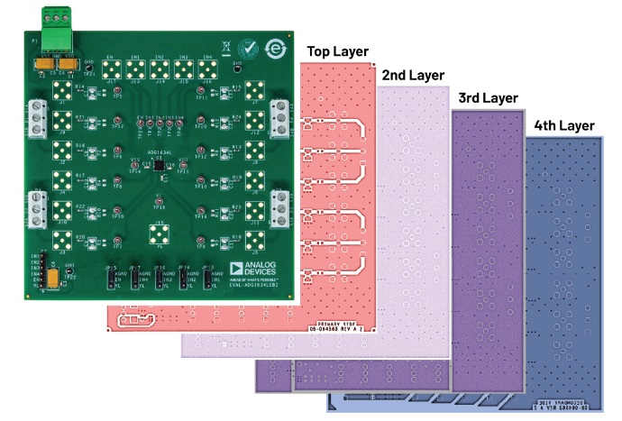
You may find that the inner layers have wider alignment widths than the outer layers because they tend to generate more heat. The outer layers will not get as much heat due to convection.
For safety reasons, it is recommended to use the entire inner PCB alignment width.
- Use of equations
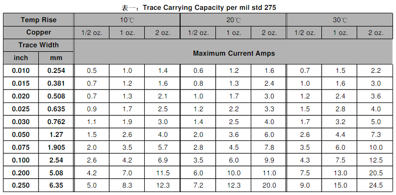
1) PCB trace width calculation table
PCB trace width calculation table can help you determine the
PCB alignment width, but also allows you to understand the impact of current-carrying capacity and temperature rise, you can refer to the following table.
2) PCB trace width formula
According to the definition of IPC 2221, you can use the formula for calculating the allowable current through the alignment to find the PCB alignment width. The process is as follows
I=kΔT^0.44A^0.725
I represents the current and is taken as a constant
ΔT is the change in temperature
A is the cross-sectional area of the alignment.
The formula can now be rearranged to derive the trace width by finding the cross-sectional area through which the chosen currency safely passes.
Area [mils^2] = (current [amps]/(k*(temperature rise [degrees Celsius])^ 0.44))^(1/0.725)
k = 0.048
Then, consider the thickness of the alignment in order to find the desired width.
Width [mils] = Area [mils^2]/(Thickness [oz]*1.378[mils/oz])
This formula can be used for currents from 0 to 35 A and allows for temperatures from 10 °C to 100 °C. The formula can be used for currents from 0 to 35 A, allowing for temperatures from 10 °C to 100 °C. It accommodates
400 mils trace width, and you can use copper values from 0.5 to 3 oz.
By plugging 2 A into the above calculation, we get at least about 30 mils of trace. But you cannot calculate the voltage drop because you need to calculate the circuit of the alignment.
The importance ofpcb trace width current in PCB layout
1.PCB Electrical Performance
The PCB trace width affects the electrical performance of the PCB, including: signal integrity and power integrity.
(1) PCB
Most digital wiring on a PCB board will use default values for trace width and spacing, but some networks require different dimensions. For example, controlled impedance networks will need to have their trace widths calculated based on the configuration of the board stack.
(2) Sensitive high-speed alignments may require larger spacing values to prevent crosstalk and other signal integrity issues.
(3) Signal integrity can be greatly improved and signal interference, crosstalk, EMI, etc. can be controlled by using different alignment widths.
(4) Depending on the purpose of the circuit, analog cabling may also require unique alignment widths and spacing. In some cases, the default alignment width may be reduced in narrow and tight areas, but care must be taken not to extend it across the board.
(5) If the alignment becomes so thin that it is compromised during PCB fabrication, the signal integrity of the entire board may be compromised.
- Power and Ground Routing
(1) The traces used to route power and ground need to be wider to conduct more current. If the traces are too thin, they can get hot or even burn through.
(2) Power traces routed to the inner layers of the board also need to be wider than those routed to the outer layers because exposure to air provides more cooling.
(3) For those alignments used in power circuits, it is important to keep the line widths as short as possible and as wide as possible to handle the current as well as to reduce inductance and noise in the circuit. It is important to increase the spacing of alignments that carry higher currents to prevent the power supply from arcing between them. - Microstrip and Ribbon Lines
For sensitive high-speed transmission lines, you need to couple the alignment to a reference ground plane in order to shield the alignment. A stripline configuration is an internal wiring layer sandwiched between two ground layers. On the other hand, a microstrip configuration refers to an alignment on the outside of the board and the adjacent planes below it. - Analog Routing
For analog signals, alignments need to be short and direct with extra width to keep alignment impedance low. For analog circuits, it is best to minimize the use of vias. - Power Integrity
(1) Short and direct routing, it is important to keep the alignment short to avoid additional noise. Rounded corners are also preferred as opposed to right angles.
(2) Use wide traces. To minimize inductance and crosstalk, it is prudent to use wide traces with power wiring.
(3) Current and heat dissipation considerations, power supply alignments conduct different current levels depending on the network being wired. In addition, it is important to consider the heat generated by the wiring with the current. Outer layers of power traces can also benefit from air cooling. - Board Manufacturing
The wider the alignment, the easier it is to manufacture. The manufacturing etching process has a greater impact on long, isolated alignments, so it is best to make them as wide as possible. A 20 mil alignment is much more tolerant of missing metal than a 3 mil alignment.
The width of the alignment also depends on the weight of the copper used to build the layers of the board, and a manufacturer may not be able to etch thinner alignment widths on that layer of the board if it requires a greater weight of copper due to higher current requirements.
- Board Assembly
Excessively wide alignments affect the ease with which electronic components can be soldered during PCB assembly.
The ease with which components can be soldered during PCB assembly.
(1) Wide alignments for power and ground grids can also act as heat sinks, resulting in uneven heating and poor solder joints.
(2) Small, two-pin components with a large area of metal attached to one pad and a thin trace attached to the other pad can be so unbalanced that the assembly will pull up during reflow, an effect known as “tombstoning,” which forces the board to be manually reworked to make corrections.
(3) BGA
The large amount of metal under the BGA can also cause problems during soldering, but due to the size of the BGA on the board, these errors are more difficult to detect.
All potential problems can occur if the correct alignment width and spacing is not maintained.
- Impedance
In some applications, impedance is another determining factor.
(1) At low frequencies (i.e., below a few megahertz), impedance is not much of an issue, and the width of the alignment can be set entirely according to current handling requirements or manufacturing process limitations.
(2) But when it comes to PCBs with higher frequency signals, the PCB connection begins to behave more like a transmission line than a simple shorted conductor, due to the fact that the high frequency signals moving along the traces create a magnetic field around the current and an electric field (charge) between the traces. In this case, controlled impedance is taken into account when the design of the PCB also includes PCBs for the trace width current.
Accurate design of PCB trace widths is critical to the safety, reliability and performance of circuits. Through the rational use of pcb trace width calculator and consider a variety of factors, designers can ensure that the alignment width not only meets the performance requirements, but also in line with the manufacturing process standards, for high-quality PCB design to lay a solid foundation.