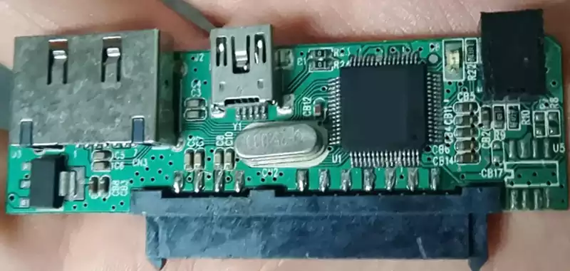
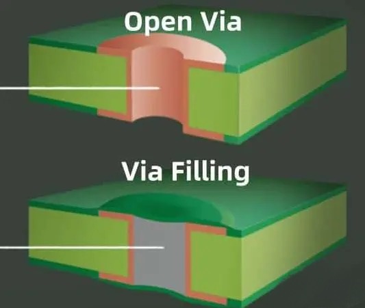
pcb via filling is a treatment of overvias during the manufacturing process of printed circuit boards (pcb), designed to improve the performance and reliability of the board. Vias are conductive pathways that connect different layers of the pcb. Through plating and filling treatments, via filling enhances the electrical performance and thermal management of the via while improving the overall reliability of the board. This filling is usually accomplished by solid conductive materials, which not only fills the voids inside the vias, but also effectively improves the thermal performance and helps reduce the operating temperature of the circuit. Types of via filling include through holes, blind holes and buried holes. Select the appropriate diameter of the via according to the diameter of the wires to be connected to ensure a good electrical connection.
In addition, the layout of the over-holes should be as uniform as possible to avoid creating uneven stresses or weak points on the pcb to improve the mechanical strength and stability of the board. The over-hole filling material can be conductive (e.g., copper) or non-conductive (e.g., epoxy paste), and the specific choice depends on the design requirements and the specific application of the circuit board. The vias plugging process is an important complement to the vias capping process and is usually used in the production of high quality pcb boards.
In the via plugging process, ink is first used to fill the entire through-hole to ensure that no light can pass through, thus preventing the ink on the soldermask ring from flowing into the hole and effectively avoiding the problem of yellowing of the over-hole. It is worth noting that the size of the hole has an important impact on the effect of oil plugging, the smaller the hole the easier it is to plug the oil, and too large a hole is not suitable for oil plugging process, generally recommended that the maximum size of no more than 0.5mm. for holes larger than 0.5mm, usually used to cover the oil hole in the way of oil processing.
The role of pcb perforation
Electrical connection: perforation is the electrical connection channel between different pcb layers, enabling signals to be transmitted between different layers. This is critical for multi-layer pcb to ensure circuit integrity and functionality.
Signal Integrity: With properly designed vias, signal loss during transmission can be reduced and signal integrity optimized.
Thermal Management: Vias can be used for thermal conduction to conduct heat from a heat source (e.g. a power component) to other areas, helping to dissipate heat and keep circuits stable.
Mechanical Support: Vias provide additional mechanical strength in some cases, enhancing the overall structure of the board. Anti-solder layer protection: Vias are designed to minimize solder inhalation during the soldering process and avoid potential soldering defects.
Classification of Vias
- According to structure and shape:
Blind Via: connects only the outer layer and inner layer, does not penetrate the whole pcb. suitable for high density layout.
Buried Via: connects the two inner layers, not connected to the outer layer. Usually used in multi-layer pcb to save space.
Through Hole: Runs through the entire pcb, connects all layers. Most common type, suitable for most basic applications.
Depending on the function:
Signal Through Hole: Used to carry signal current, usually designed to be as small as possible to minimize signal delay.
Power vias: used exclusively to carry power and may require larger hole diameters and better filler materials to carry higher currents.
Ground Vias: Used to connect to a ground plane to reduce noise and improve electrical performance.
Depending on the filler material:
Filled Vias: Vias filled with resin, metal or conductive adhesive to improve electrical performance and mechanical strength.
Unfilled Vias: Vias without any filling material, suitable for simple electrical connections.
Depending on the application scenario:
High Frequency Application Vias: Designed to be exceptionally small to reduce parasitic capacitance and inductance, suitable for RF circuits.
High power application vias: designed to be larger and use higher strength materials to carry higher currents.
Through-hole windowing
Through-hole windowing means that the through-hole pads are not covered with ink, exposing the copper surface, which is surface-treated to create a sunken gold or sprayed tin effect. The main role of this process is in the components over the wave soldering, spray tin can fill the hole wall, thus increasing the hole’s ability to conduct current. The effect of via windowing is similar to that of plug-in holes, so there is no need to remove the via windowing when converting a Gerber file.
The through-hole windowing process is suitable for applications that require high through-current capability, such as circuit boards for high-power electronic devices. It also improves the solderability and reliability of circuit boards.
Oil Plugging
The process of oil plugging refers to the filling of ink inside the walls of the apertures. In this process, an aluminum sheet is used to plug the soldermask into the apertures first, and then the entire board is printed with soldermask. The main purpose of plugging the vias with solder resist is to prevent short-circuiting of the HDI when it is wave-soldered with tin running through the vias to the component face.
When converting the design file to a Gerber file, it is also necessary to eliminate the windowing of the vias. The vias plugging process improves the insulation and short circuit resistance of the board, and is especially suitable for high density and high reliability board manufacturing.
Resin plugging refers to filling the inside of the via hole walls with resin, followed by pad leveling. This process is applicable to any type of one-sided windowed vias or two-sided windowed holes in the disk. The main purpose of resin plugging holes is to prevent the PP adhesive from flowing into the holes during the pressing process, resulting in a lack of adhesive in the laminate to explode the board, and also to increase the soldering area of the pads to improve the reliability of the soldering.
When the design file is converted to a Gerber file, it is necessary to cancel the windowing of the vias. Resin plug hole process has significant advantages in improving the mechanical strength and electrical performance of the circuit board, especially for the circuit board performance requirements of high application scenarios.
Vias in pcb mainly play the role of interlayer conduction. In order to avoid short circuits and other problems in the process of use, usually used to cover the oil way to deal with, not only to ensure the stability of the electrical properties, but also reduces the risk of short circuits with other components. However, in some special cases, such as the need to use the over-hole as a test point or heat dissipation channel, the window will be used to deal with the way.
In pcb via filling, the commonly used filling materials mainly include the following:
Resin:
Epoxy resin: common and has good insulation properties and mechanical strength for most applications. Epoxy-based materials are widely used and versatile. Applications include coatings, adhesives and (such as carbon and glass fiber reinforced) composites. The chemistry of epoxy resins and the variety of commercially available variants give the cured polymers a very wide range of properties. In general, epoxy resins are known for their excellent adhesion, chemical and heat resistance, good to excellent mechanical properties, and excellent electrical insulation properties.
Polyester resins: High temperature resistant and suitable for specific high temperature environments. Polyester resins are a substance that can be used in a variety of ways, including the construction of boats, the manufacture of different parts in models, or in the production of ponds and swimming pools. Polyester resins can also be used to make fiber composites, also known as thermosets. They differ from thermoplastics because they are not flexible and cannot be welded. There are two main types of polyester resins: slow-curing and fast-curing.
Metal:
Copper-filled: copper filling of the perforations by plating or other means can significantly improve electrical conductivity and heat dissipation.
ALUMINUM FILLING: Aluminum is also an option in some specific applications.
Conductive Fillers:
Conductive Adhesives: Conductive adhesives can be used in the perforations for applications requiring good conductivity.
Silver or Carbon Fillers: Enhance conductivity while also providing some mechanical strength.
Other materials:
Ceramic or composite materials: for special applications requiring high insulation or high temperature resistance.
When selecting filler materials, it is necessary to consider the electrical properties, thermal properties, cost and the feasibility of the manufacturing process to meet the specific application requirements
Processes for pcb via filling
There are three main processes for over-hole filling: tented over-hole, uncovered over-hole and inserted over-hole with soldermask. Each process has its own characteristics and applicable scenarios.
Tented via: A tent-like protective layer is formed over the via to prevent solder bridging.
Covered Vias: The vias are completely exposed and are suitable for applications that require heat dissipation through the vias or special electrical properties.
Solder Resist Inserted Vias: A solder resist layer is formed around the via to prevent solder penetration while providing additional protection.
Five advantages of pcb via filling
- Electrical performance enhancement: Hole filling reduces short cut-off line resonance, lowers impedance discontinuities, reduces reflection and insertion losses, and maintains high frequency signal integrity.
- Thermal management optimization: filler material improves the thermal conductivity of the vias, helping to dissipate heat in multilayer pcb and manage heat in high-current vias.
- Reliability enhancement: Vias filling improves the reliability of connections by strengthening them and reducing the risk of cracking due to thermal stress.
- Noise and crosstalk reduction: Filler materials help reduce noise and crosstalk in circuits, improving signal clarity.
- Manufacturability enhancement: Allows for higher through-hole aspect ratios, realizing smaller through-hole sizes and simplifying the process of covering and tenting through-holes.
The impact of over-hole filling on pcb reliability
- Stability of electrical connections: Over-hole filling provides more stable electrical connections and reduces circuit failures due to through-hole breakage or poor contact.
- Thermal cycling tolerance: During thermal cycling, the thermal expansion coefficient of the over-hole filling material matches that of the pcb material, reducing cracking due to thermal stress.
- Long-term operational reliability: the durability of the perforated filler material ensures that the pcb will not be damaged in the long term.
pcb via filling, although seemingly insignificant, is a key technology to ensure pcb reliability. It not only improves electrical performance and optimizes thermal management, but also enhances overall reliability and manufacturability. Overvias provide a more stable and reliable operating environment for our electronic devices.