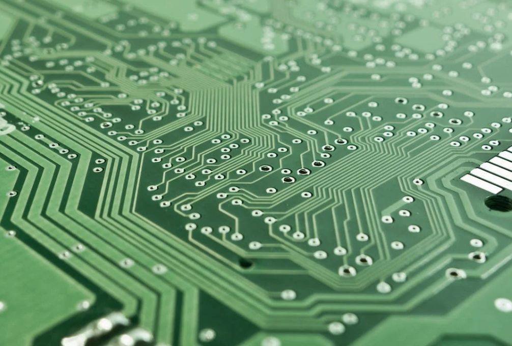
In the PCB manufacturing process, pcb warpage problem has been one of the key factors affecting product quality and productivity. Warped PCB boards are not only difficult to subsequent assembly and soldering, but may also be rejected because they do not meet the specifications, leading to increased production costs and delivery delays. In order to effectively solve this problem, PCB manufacturers continue to explore and practice various warpage repair methods.
PCB warpage repair methods
1.PCB production process of warping correction: in the PCB production process, for the warping degree of the larger plate, will use the roller levelling machine for screening and levelling treatment, and then these plates will continue to enter the subsequent production process. Many PCB manufacturers agree that this step has a positive effect on reducing the PCB warpage.
2.In response to the apparent warpage of the finished PCB boards, some manufacturers use small presses (or similar clamping devices) to perform cold press corrections to keep the PCB boards in the device for several hours to several dozen hours, as roll levelling machines are not suitable. However, this method has proven to be of limited effectiveness. On the one hand, the levelling effect is not significant; on the other hand, after correction of the PCB board is easy to return to the original warped state. Some PCB factories try to small presses heated to a certain temperature, the implementation of hot pressing of PCB boards, although the effect is better than cold pressing, but too much pressure may cause deformation of the wire, while too high a temperature may lead to rosin discolouration and other issues. Whether cold or hot pressing, it takes a considerable amount of time (hours to tens of hours) before a certain effect can be observed, and the corrected PCB board has a high warpage rebound rate.
A hot stamping flattening technique using a bow mould is presented here. Depending on the area of the PCB to be flattened, we can customize a simple bow mould (as shown in Fig. 1). Next, we propose two methods of levelling operations:

(1) Baking flattening method using the combination of bow mould and oven: firstly, the curved surface of the warped PCB board is fitted with the curved surface of the bow mould,and the PCB board is pre-deformed in the opposite direction by adjusting the fixture screws. Then, the whole mould together with the PCB board is put into the oven and heated to a certain temperature for baking.Under the effect of heating, the stress inside the substrate will gradually be relaxed, so that the original deformation of the PCB board to restore flatness.It is worth noting that the baking temperature needs to be controlled within a certain range, to avoid too high leading to rosin discolouration or yellowing of the substrate,and at the same time should not be too low, because the stress relaxation at low temperatures takes longer. Usually, the glass transition temperature of the substrate can be used as a reference for the baking temperature because it is the phase change point of the resin, at which the polymer chain segments can be rearranged to ensure that the substrate stresses are fully relaxed. This method of levelling is highly effective and less costly using bow moulds. It is also very easy to operate as ovens are commonly available in PCB factories. If the number of PCBs to be flattened is large, only a few bow moulds need to be made. They can be put into the oven at once,due to the small number of moulds, baking time is relatively short (only a few minutes or so), so the leveling work efficiency is high.
(2) PCB board softening bow mould flattening process: for the small degree of the PCB warpage,we use the first softening after flattening method. Specific operation is,the PCB board to be flattened in the preheating to a specific temperature in the oven (the temperature is based on the substrate’s glass transition temperature to set the baking time should be based on the substrate softening to determine the situation. Usually, the glass fibre cloth substrate requires a higher baking temperature, while the paper substrate is relatively low; thick boards can be baked at a slightly higher temperature, while thin boards are slightly lower. For PCBs that have been sprayed with rosin, the baking temperature should be avoided. After baking for a period of time, take out several to more than ten PCB boards, quickly clamped into the bow-shaped mould, and by adjusting the pressure screws to make it slightly reverse warping to offset the original deformation. PCB board to be cooled and shaped, can be removed from the mould, at this time the PCB board has reached a flat state. After the use of bow mould flattening PCB warping degree is very low, even after wave soldering can also maintain good flatness, and the PCB board appearance of the colour of the impact is minimal. PCB board warping has been plagued by manufacturers of the problem, it will not only reduce production efficiency, but also delay the delivery date. The use of reasonable bow mould thermal leveling process can effectively solve this problem, to ensure that the warped PCB boards can be leveled to meet the requirements of the delivery date.
Bow mould hot stamping and flattening technology with its unique advantages, in the field of PCB warpage repair shine. Through precise control and efficient operation, this technology not only solves the problem of PCB warpage, which has plagued manufacturers for a long time, but also opens up a new way to improve product quality and production efficiency. Looking ahead, the technology will continue to be optimised, contributing to the prosperity of the PCB manufacturing industry.