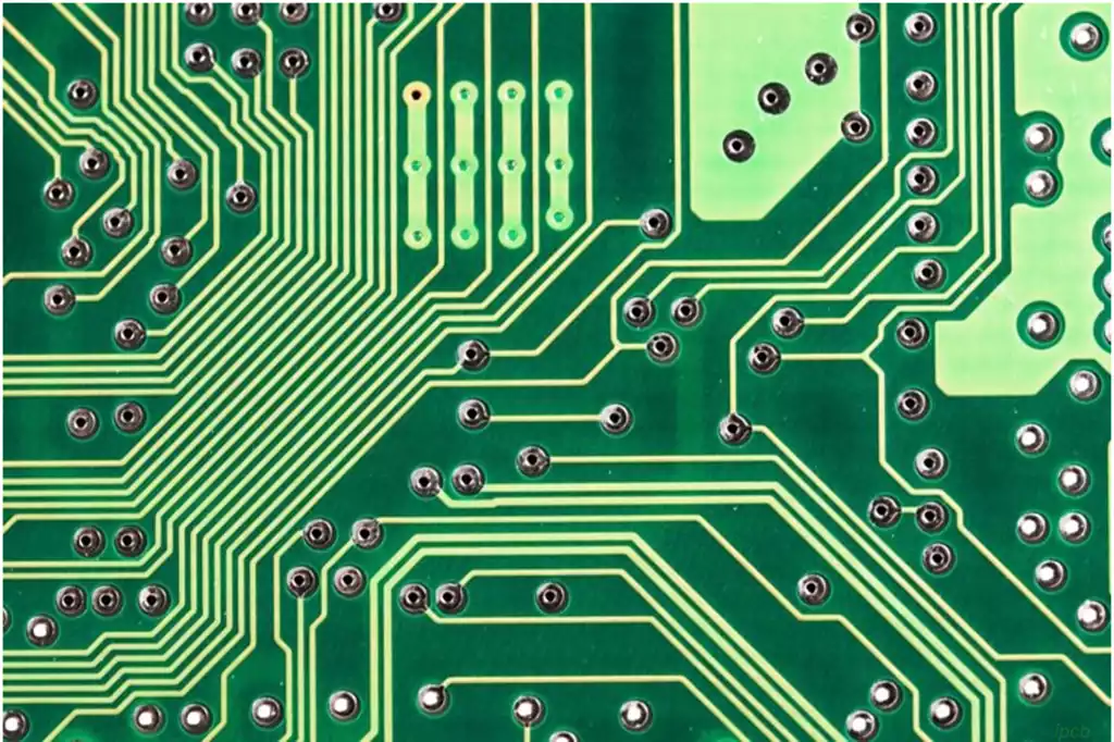
Plated Through Hole (PTH) is a key process in the manufacture of printed circuit boards, the main role is to chemically deposit a thin layer of copper on the insulating substrate inside the hole, to provide a conductive layer for the subsequent plating, so as to achieve the role of the inner and outer layers of the conductive.
The implementation process of PTH technology includes the steps of drilling, hole wall cleaning and pretreatment, conductive thin layer deposition, and plating.
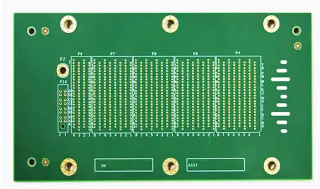
Drilling is the starting point for PTH technology. Precise drilling of the desired holes in the PCB lays the foundation for subsequent metal deposition. This step requires high-precision drilling equipment to ensure that the position and size of each hole is accurate.
The next step is hole wall cleaning and pre-treatment. The purpose of this step is to remove impurities and oil from the hole walls, creating a clean environment for subsequent metal deposition. With special cleaning agents and treatments, the hole walls are made smooth and clean, ready for the next steps.
Then the deposition of the conductive thin layer begins. In this step, the walls of the holes are coated with a thin conductive layer, usually copper or another metal. This conductive layer will serve as a seed layer of metal for subsequent plating, ensuring that the metal will be evenly deposited on the hole wall.
The final step is plating. In this step, the board is immersed in a plating solution containing metal ions. Through the action of an electric current, the metal ions are reduced to metal on the walls of the holes, forming a conductive metal layer. This process requires precise control of the current and plating time to ensure that the thickness and conductivity of the metal layer meets the requirements.
Plated Through Hole (PTH) for printed circuit boards plays a crucial role in electronics manufacturing. This technology not only affects the design and manufacturing process of the board, but also directly relates to the performance and reliability of the final product.
Interconnecting circuits: Interconnections between different circuit layers are realized by depositing conductive metals on the walls of the holes in the circuit board. This is fundamental to the proper functioning of electronic devices, as it allows current to flow between different circuit components.
Enhanced reliability of the board: Since the PTH process creates a solid metal layer on the hole walls, this increases the mechanical strength of the board. This means that the circuit boards are able to resist external physical stresses such as vibration, shock, etc., thus increasing the reliability and durability of the product.
Improved conductivity of the board: The presence of the metal layer significantly improves the conductivity of the pcb board. It lowers the electrical resistance, allowing current to flow more smoothly through the board, reducing energy loss and heat generation.
Supports High Power and High Temperature Applications: The PTH process is capable of producing boards that can withstand high power and high temperatures. This makes it particularly suitable for electronic devices that need to withstand extreme operating environments, such as aerospace and military products.
Facilitates production automation: The standardization and repeatability of PTH technology makes the production of electronic devices more automated and efficient. It reduces manufacturing costs and increases productivity, making electronic devices more popular and cheaper.
Plated Through Hole technology is a key technology in printed circuit board manufacturing. Its application not only improves the performance and reliability of circuit boards, but also provides a solid guarantee for the normal operation of electronic equipment.