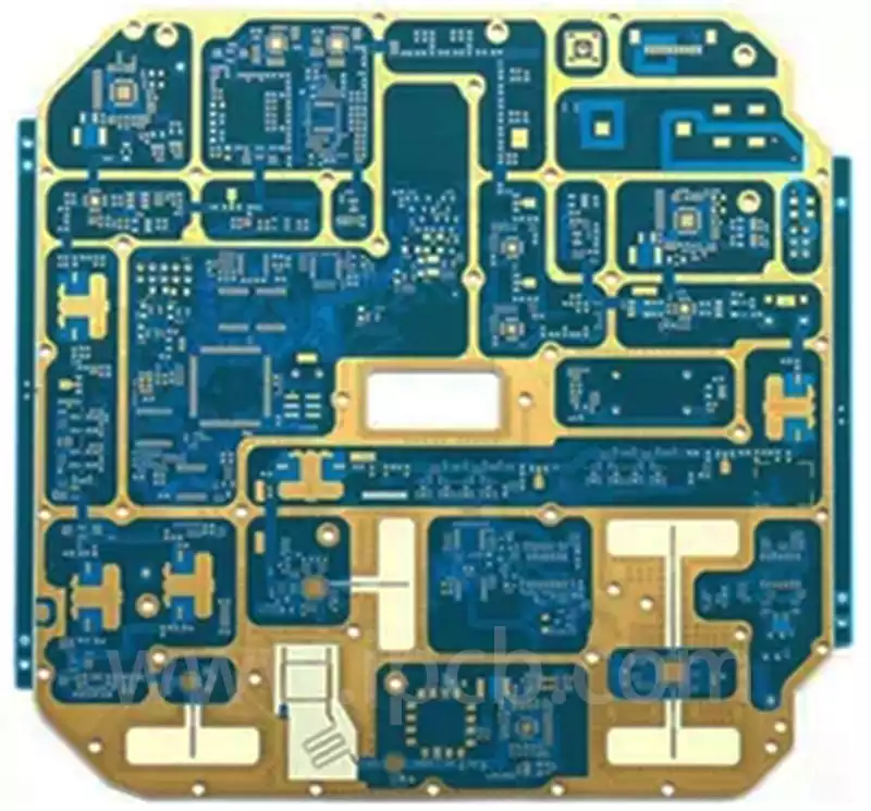
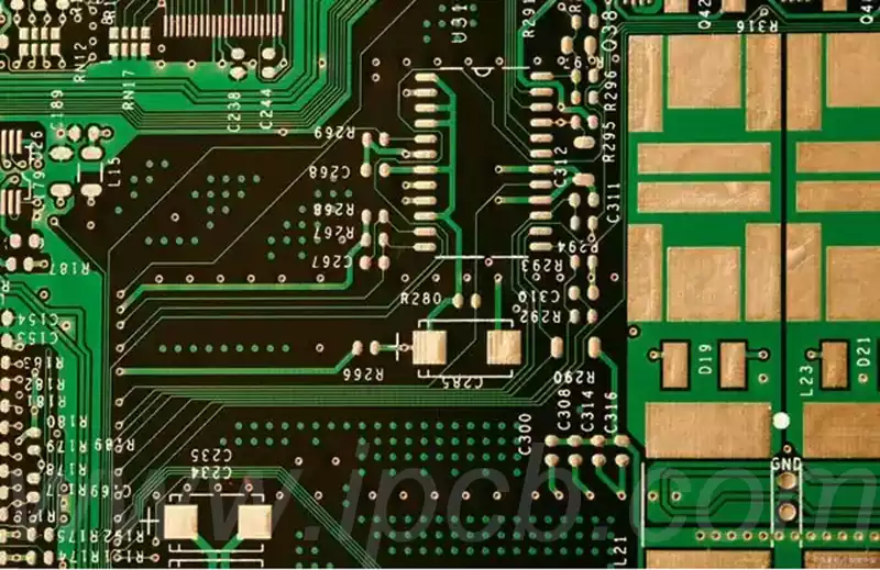
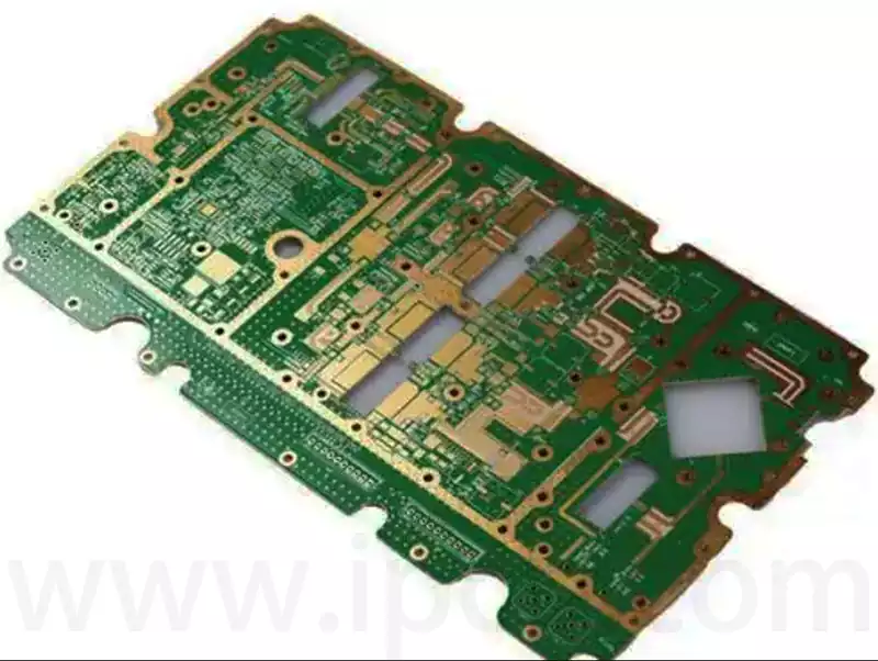
In the mass production of printed circuit boards (PCBs), manufacturers often combine multiple individual boards into one large board, a process known as boardmixing, where multiple small boards are combined into one large board. The aim is to feed these boards more efficiently into the automated machines of the SMT (surface mount technology) production line, thereby increasing overall productivity and reducing the amount of time that expensive production equipment has to sit idle while waiting. However, when designing these boards, engineers also need to consider very carefully how to separate them conveniently, that is, the process of splitting the boards, in order to avoid the embarrassing situation that although it is easy to put the boards together, it is difficult to split the boards.
PCB Design Methods.
V cut, also known as V-groove cut or V-groove cut, is a technique used for layering in the production of multilayer PCBs. The specific operation is to pre-design a V-shaped groove between two adjacent layers of PCB boards, and cut this V-shaped groove on the edge of the board by laser or mechanical processing. When the entire multilayer board is finished with all layers pressed together, the multilayer board can be precisely separated into individual boards along these V-grooves.
Advantages: High accuracy: The V cut ensures neat edges after layering, making it suitable for applications with strict requirements for accuracy. Aesthetically pleasing: The cut surface is flat, enhancing the overall aesthetics of the product. Suitable for automated production: Easy to be gripped and handled by automated equipment.
Disadvantages: Strength limitation: the strength of V cut edge is relatively low, which may not be suitable for applications that need to withstand large mechanical stress. Layer limitations: For PCBs exceeding a certain number of layers, V-cut depth control becomes more difficult and may affect the quality of the finished product.
PCB stamp holes are holes in the motherboard faceplate that are used to connect the small PCBs that make up the array together, allowing you to easily remove components from the PCB. The stamp holes are perforated and break when you push down, allowing you to remove components without damaging the PCB itself.
What PCB Stamp Holes Do PCBs are designed with stamp holes for a number of reasons:
1.Can connect small PCB boards into a group When you have a bunch of PCBs that need to be connected and are too small to use connectors, you can use stamp hole’s to connect them. The perforations will allow current to flow through the PCB and connect to other PCBs nearby.
2.Can transfer power and data between two different PCBs/devices If you need a device to communicate with another device, you can use stamp holes.
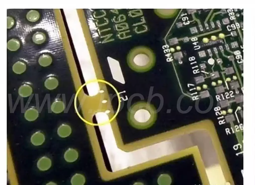
PCB Stamp Hole Design Requirements
1.PCB Stamp Hole
The number of holes stamp holes are usually in groups of 5 and are used to connect components together and may vary depending on the PCB design.
2.PCB Stamp Hole Size
PCB stamp hole size is usually 0.020 inches or 0.5 mm in diameter and may vary depending on the PCB design.The PCB stamp hole size is determined by the thickness of the material used to manufacture the PCB.
3.PCB Stamp Hole Pitch
Typically, PCB stamp holes are spaced 0.030 inches or 0.76 mm apart, which prevents components from being too close together and causing short circuits.
Comparison of the differences between PCB stamp holes and V-grooves
V-Groove Overview: V-Grooves are an extremely common connection in the PCB assembly process, V-CUT technology allows us to combine several boards, or different parts of the same board, together. After the PCB has been processed, a V-CUT machine is used to cut the V-grooves between the boards so that they can be easily broken during use or before packaging. When double-sided V-groove design is used, it is necessary to ensure that the depth of the V-groove is controlled to be about 1/3 of the sum of the grooves on both sides, and at the same time to ensure that the groove size is accurate and the depth is uniform.
Advantages of V cut:
Cost-effective: the production cost of V-groove is relatively low.
Easy to manufacture: the manufacturing process is relatively simple and fast.
Stable quality: V-groove is not easy to deform, to ensure the quality of the product.
Application of PCB stamp holes: In many PCB designs, stamp holes are used as an alternative to V-grooves.
Advantages of stamp holes:
Strength Enhancement: The connection method of stamp holes makes them stronger and can be broken directly by hand or tools without relying on complex equipment such as milling machines.
Enhanced Grip: The design of the stamp holes increases the surface area of the adhesive in contact with the PCB, thus providing a stronger grip, making the installation more stable while effectively preventing the PCB from moving.
Reasons for and Advantages of PCB Patchwork
Why do you need to carry out the operation of board-splicing? The benefits brought by board-splicing:
Adapt to the production demand: some PCB board size is too small to meet the requirements of the use of fixtures, so it is necessary to combine them through the way of board assembly for production.
Enhance SMT soldering efficiency: With the patchwork board method, the soldering of multiple PCB boards can be completed through only one SMT process, which significantly improves the production efficiency.
Optimise cost utilisation: For irregularly shaped PCBs, PCB assembly can make more effective use of the board area and reduce material waste, thus improving cost efficiency.
V cut Depaneling Methods
The standard way to depanel V-notch PCBs is to use a V-notch depaneling machine, which is mainly applicable to PCBs with V-cut. Additionally, board fishing machines, laser cutters and manual methods can also be used for parting operations.
As a rule, the residual thickness of the V-notch is retained at about one-third of the board thickness, which prevents accidental breakage during the production process and allows for easy depanelling when required.
V-shaped groove connecting plate is designed to facilitate the operator to manually divide the board. At the beginning of PCBA soldering assembly, mainly wave soldering of through-hole parts (THDs), these parts have high solder strength, so the bending stress during depaneling has less impact on them. However, with the introduction of Surface Mounted Soldering (SMA) Sticky Soldered Parts (SMDs), the bending of the board due to stress may lead to tin cracks and rupture of the soldered parts, and therefore manual methods of depaneling are no longer recommended.
Stamp Hole Depaneling Methods
Stamp holes are conceived as a row of small holes (stamp holes) punched into the veneer at both ends of the bar to facilitate manual depaneling with tools such as diagonal pliers. Therefore, stamp holes are usually used in scenarios such as prototyping, small batch production or home substitution. Of course, when needed, stamp holes can also be regarded as connecting ribs and used for depaneling operations using board fishing machines or laser cutting machines.
V-cut and stamp holes have their own unique advantages and application scenarios in PCB board splitting technology, and V-groove has become the first choice for mass production due to its low cost, easy to manufacture, and stable quality. Stamp holes, on the other hand, show their irreplaceability in situations that require higher strength, greater grip or special design needs. Either way, it is necessary to fully consider the production process, equipment capacity and product quality requirements in the design of the collocation board, in order to ensure the reliability of the final product and production efficiency. With the continuous progress of electronic manufacturing technology, PCB PCB sub-board technology will also continue to innovate and develop, for the miniaturisation of electronic products, integration and efficient production to provide more possibilities.
