In electronic circuit design, pcb circuit board line width is closely related to its current carrying capacity. Wire width directly determines the cross-sectional area of the wire, thus affecting the maximum current it can withstand. The proper design of the line width not only ensures the normal operation and safety of the circuit, but also improves the overall thermal management.
Relationship Between pcb circuit Board Wire Width and Current Carrying Capacity
Effect of Wire Width on Current Carrying Capacity
The wider the wire width on a pcb circuit board, the more current it can carry. This is because wider wires provide a larger cross-sectional area, which allows more electrons to pass through. When there is too much current, if the wire width is insufficient, the wire may be damaged by overheating or even cause a fire. Therefore, when designing circuit boards, engineers need to set the wire width properly according to the expected current load.
The Importance of Reasonable Line Width Design
Reasonable line width design not only improves the current carrying capacity of a pcb circuit board, but also enhances its safety and stability. Too narrow a line width can lead to excessive current density, which can lead to thermal failure of the board. Too wide a line width can waste material costs and take up too much space. Therefore, finding a balance is critical.
Recommendations for Optimising Line Width and Current Carrying Capacity
To optimise the relationship between line width and current carrying capacity of a circuit board, engineers can take the following steps:
- set the line width according to the current load and board space.
- use highly conductive materials.
- use highly conductive materials to improve the efficiency of current transfer.
- if necessary, multi-layer board design can be used to increase the wiring space.
PCB circuit board current-carrying capacity calculation
The current-carrying capacity of the PCB circuit board depends on the alignment line width, limiting current and other factors. Here are some commonly used PCB current-carrying capacity calculation methods.
1. Film thickness calculation method
film thickness calculation method is a common method to estimate the current-carrying capacity of the PCB circuit board. Through the film thickness calculation method can roughly estimate the current-carrying capacity of the PCB, and according to the standard indicators to adjust the PCB alignment line width and current limit.
2.Error method
Error method is a more accurate method of calculating PCB current-carrying capacity. This method needs to be carried out through the actual PCB production and testing. First of all need to determine the electronic components of the PCB, and then PCB circuit board production and testing, according to the actual test results of the PCB alignment adjustment.
3.Simulation method
Simulation method is a commonly used method in PCB design, can be electromagnetic simulation to simulate the circuit state of the PCB board. Through the simulation method can more accurately estimate the current-carrying capacity of the PCB circuit board, and according to the simulation results of the PCB alignment adjustments to enhance the current-carrying capacity of the PCB circuit board.
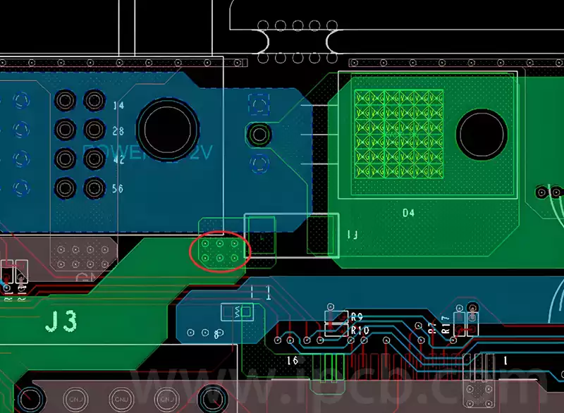
Factors affecting the current-carrying capacity of the PCB conductor:
PCB conductor current under the same conditions, the higher the current, the higher the temperature rise, the current-carrying capacity decreases.
PCB conductor width of the same cross-sectional area, the wider the wire, the better the heat dissipation, the better the current-carrying capacity.
PCB conductor thickness of the same cross-sectional area, the thinner the conductor copper thickness, the better the heat dissipation, 1oz temperature rise than 0.5oz 5~10%, 2oz temperature rise than 1oz 10~15%, 3oz temperature rise than 2oz 15~20%.
PCB board thickness board thickness affects the heat transfer path, the thicker the board, the better the heat dissipation. The same FR-4 plate, 0.965mm plate thickness than 1.79mm plate thickness, the conductor temperature rise out of 30-40%.
PCB sheet plate thermal conductivity directly affects the conductor temperature rise, the greater the thermal conductivity, the lower the conductor temperature rise. The thermal conductivity of copper is about 1000 times that of FR-4 sheet, and the thermal conductivity of FR-4 sheet is 10 times that of still air. Therefore, under the condition of static air, the temperature rise of the conductor inside the PCB circuit board will be less than that of the external conductor.
The same layer of adjacent conductors in the same layer of the conductor near, if there are other conductors, the heat dissipation effect will be reduced, the more the number of roots of the same layer of adjacent conductors, the worse the heat dissipation, the higher the temperature rise, the current-carrying capacity decreases.
Adjacent layer of copper plane adjacent layer of copper plane on the conductor temperature rise has the greatest impact. Whether it is the power plane, ground plane, or other copper planes, it helps dissipate heat and thus reduces the temperature rise. Conductor to the adjacent layer of copper plane the closer the distance, the lower the temperature rise of the conductor; adjacent layer of copper plane area the larger, the lower the temperature rise of the conductor; adjacent layer of copper plane the thicker, the lower the temperature rise of the conductor; adjacent layer of copper plane the more the number of the conductor temperature rise, the lower the temperature rise of the conductor.
Surface coating PCB surface solder resist paint coating, will also affect the conductor heat dissipation effect, the thicker the coating, the worse the heat dissipation effect, the higher the temperature rise.
Reasonable set of PCB circuit board alignment line width to enhance the current-carrying capacity of the circuit board and the overall performance is of great significance. During the design process, it is necessary to take into account a variety of factors, such as wire width, copper thickness, board properties and ambient temperature, in order to achieve the best balance between current-carrying and heat dissipation. Through film thickness calculations, error testing and simulation analysis, designers can accurately assess and optimise the current-carrying capacity of PCBs to ensure the safe and stable operation of circuits in real-world applications.
