The fundamentals of RF circuit design include:
- Impedance matching Q: Impedance matching is the process of matching the output impedance of a signal source to the input impedance of a load to maximise power transfer. This is usually achieved by using a matching network or tuner to match the impedance of the source and the load.
- Tuning: Tuning refers to changing the resonant frequency of a circuit by changing the parameters of the circuit components (e.g. inductance or capacitance). Tuning can be used to select signals in a particular frequency band or to optimise the performance of a circuit.
- Filtering:Filtering is the process of selecting appropriate circuit components to attenuate or block unwanted frequency components in order to retain the desired signal. Common filters include low-pass, high-pass, band-pass, and band-stop filters.
- Amplifier Design:Amplifiers are circuit elements used to increase signal strength. Amplifier design considers factors such as gain, stability, noise, and linearity. Common types of amplifiers include unipolar transistor (BJT) amplifiers and field effect transistor (FET) amplifiers.
- Mixing:Mixing is the process of mixing two signals of different frequencies to create a new frequency component. This is commonly used in frequency conversion and down-conversion circuits.
- Oscillator Design: An oscillator is a circuit element used to generate a stable continuous wave signal. Oscillator design takes into account factors such as frequency stability, resonator quality factor and phase noise. Common types of oscillators include crystal oscillators, resonator oscillators and amplifier oscillators.
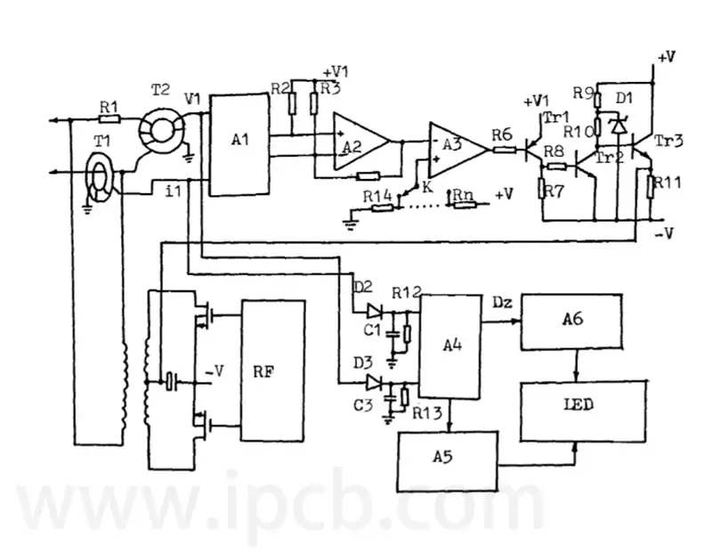
RF Circuit Layout Principles
When designing an RF layout, priority must be given to meeting the following general principles:
(1) As far as possible to isolate the high-power RF amplifier (HPA) and low-noise amplifier (LNA), in short, is to keep high-power RF transmitter circuits away from low-power RF receiver circuits;.
(2) Ensure that there is at least one block of land in the high-power area of the PCB board, preferably with no vias, and of course, the larger the copper foil area, the better; (3) The chip and power supply are decoupled from each other.
(3) chip and power supply decoupling is also extremely important; (4) RF outputs usually need to be
(4) RF outputs usually need to be far away from the RF input; (5) sensitive analogue signals should be
(5) Sensitive analogue signals should be kept as far away as possible from high-speed digital signals and RF signals.
Tuning
Tuning is an important part of RF circuit design to improve the performance of a circuit and make it better suited to a particular application. The following are some of the common methods of designing tuned circuits.
a. Changing inductance and capacitance values: Tuned circuits need to change their resonant frequency by changing the inductance and capacitance values. By adjusting the values of the inductance and capacitance, the resonant frequency of the circuit can be selected to meet the needs of a particular application. It is usually necessary to tune the circuit several times according to its characteristics and performance requirements until the optimum resonant frequency is obtained.
b. Adjusting the circuit structure: Tuning can also be achieved by changing the structure of the circuit. For example, changing the length or diameter of the circuit’s resonator can change its resonant frequency. In addition, adjusting the coupling and inductor/capacitor arrangement of the circuit can also affect the resonance frequency.
c. Selection of suitable components: In order to achieve optimum tuning, it is necessary to select suitable inductors and capacitors. The parameters of inductors and capacitors include capacitance value, inductance value, Q value, etc., which need to be selected according to the requirements of the application. For example, inductors and capacitors with high Q values can achieve better tuning performance. In addition, high-frequency components that can withstand the high-frequency signals in the circuit need to be selected.
d. Using a tuner: A tuner is a common tuning design tool that can be used to tune a circuit by adjusting its internal inductors and capacitors. The internal circuitry of a tuner includes a resonant circuit and a converter circuit that can change the impedance and resonant frequency of the circuit to achieve tuning.
Amplifier Design Essentials
In the RF circuit design system, the amplifier is an indispensable key module, its core role is to amplify the amplitude of the input signal to enhance the signal energy level. The following are some common amplifier design ideas and methods:
a. Accurate control of gain indicators: gain as a measure of amplifier performance as one of the key parameters of the signal amplification effect plays a decisive role, need to be based on the specific application scenarios for reasonable settings. In the engineering field, gain is generally measured in decibels (dB), a quantitative unit, in order to more intuitively assess the amplifier’s signal enhancement capabilities.
b. Scientific selection of topology: Common topology types of amplifiers include common emitter amplifier, common base amplifier and common collector amplifier. Different topologies have significant differences in circuit characteristics, application advantages, and potential defects, etc. In the actual design process, the most suitable topology should be selected after weighing the application requirements closely.
c. Careful selection of core components: amplifiers are usually composed of transistors, diodes and power amplifier modules. The reasonable selection of components is directly related to the performance of the amplifier, and the appropriate components should be carefully selected according to the specific application requirements. For example, if dealing with high-frequency signals, components with high-frequency response should be used; if pursuing high gain or high power output, components with corresponding characteristics should be selected accordingly.
d. Fine tuning of key parameters: The performance parameters of the amplifier cover input and output impedance, gain, bandwidth and other dimensions. In order to ensure that the amplifier achieves the best performance in the actual application, these parameters need to be carefully adjusted according to the specific application requirements. Usually, it is necessary to use the response curve analysis of the circuit, through multiple parameter optimisation and testing, gradually approaching the optimal amplification effect, so as to meet the needs of signal amplification in different application scenarios.
Mixing Technology
In the field of RF circuit design, the mixer occupies a pivotal position, its main function is to mix the different frequency components contained in the input signal, and then generate a completely new frequency components. The following are some common ways to design a mixer:
a. Selection of mixer type: Currently, the mainstream mixer types include lumped mixer, balanced mixer, and double balanced mixer, etc. Different types of mixers have their own unique characteristics. Different types of mixers have their own unique performance characteristics and advantages and disadvantages, in the actual application, according to the specific application requirements to select the most appropriate type.
b. Selection of mixer components: mixers are generally composed of diodes, MOSFETs and integrated circuits and other components. In the component selection process, must be closely integrated with the application requirements, select the appropriate components. For example, if the processing of high-frequency signals, it is necessary to select components that can withstand high-frequency operation; if the pursuit of excellent mixing performance, it should be selected with the corresponding characteristics of the components.
c. Determination of the mixer’s fundamental frequency and input frequency: The fundamental frequency of the mixer plays a central role in the process of generating a new frequency. Proper selection of the fundamental frequency and input frequency can successfully generate the desired new frequency. The difference between the fundamental frequency and the input frequency is defined as the conversion gain of the mixer, and in practice, the appropriate difference should be selected according to the specific needs.
d. Optimisation of mixer parameters: The parameters of the mixer include input and output impedance, conversion gain, bandwidth and so on. In order to meet the actual application requirements, these parameters need to be precisely adjusted. Usually, according to the response curve of the circuit, it is necessary to carry out several detailed parameter adjustments until the best mixing effect is achieved.
RF circuit design points:
- Precautions for component packaging in RF circuits
Successful RF design must pay careful attention to each step of the entire rf circuit design process and each detail, which means that the beginning of the design phase must be thorough, careful planning, and comprehensive and continuous assessment of the progress of each design step. This kind of meticulous design skills is exactly what is lacking in the culture of most domestic electronics companies. - Circuit Board Stacking (PCB Stack Up)
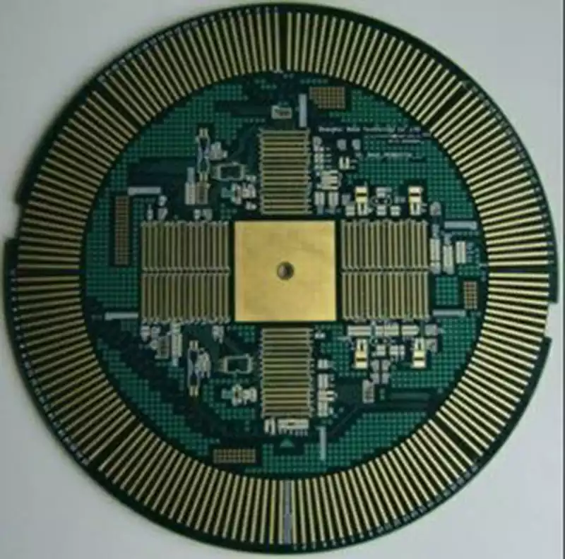
In the wiring, we must first determine the circuit board stack up, just like building a house to have the walls of the house. The determination of the circuit board stack up with the complexity of the circuit design, electromagnetic compatibility considerations and many other factors. The figure below shows the common stack-ups for four, six and eight layer boards.
Issues to be noted in the design of two-layer boards.
In a four-layer board design, we generally use the second layer as a complete ground plane, and also route important signal lines on the top layer (including RF alignments, of course) for good impedance control. In a six or more layer board design, we will also use the second layer as a complete ground plane, and then walk the most important signal lines on the top layer.
- Vias Placement
The placement of the vias is a really complicated matter. First of all, the RF alignment of the ground next to the best through the perforation, to the bottom or middle layer of the ground plane, so that any interference signal or radiation can have the shortest path to the ground, but the distance between the perforation and the RF signal line can not be too close, otherwise it will seriously affect the quality of RF signals, in the actual design process can be flexible to grasp.
Secondly, at a large area of ground plane, we usually place a lot of vias for connecting different layers of ground. This is in the RF circuit wiring, it should be noted that the large over-hole to be played without regularity, it is best to get into a diamond-shaped, which can maximise the suppression of various types of interference.
RF circuit design is a set of theoretical depth and practical precision in one of the complex engineering, its principles, layout and key module design interlocking. From the core principle of accurate control, to the layout of the rules of strict compliance, and then to the details of the elements of the fine sculpture, only the whole process of excellence, can cast high-performance, anti-interference RF circuit, for wireless communications, radar detection and other cutting-edge technologies to build a solid foundation, driving the electronics industry to higher frequency bands, stronger function of the continuous evolution.