In modern circuit design, the problem of signal interference is undoubtedly a core issue, which directly determines the performance and reliability of the entire system. For PCB engineers, signal interference design is a crucial skill and challenge. In practice, we found that there are four main sources of interference in PCB design: power supply noise, transmission line interference, coupling interference and electromagnetic interference.
Power supply noise is particularly prominent in high-frequency circuits, and its impact on high-frequency signals is very significant. Therefore, the first task is to ensure that the power supply has low noise characteristics. Again, a clean grounding environment is as important as a clean power supply.
The problem of transmission lines in the circuit board should not be ignored. Transmission lines are mainly reflections, reflections not only increase the difficulty of signal analysis, but also may cause return loss, the impact and additive noise interference is no different.
Coupling interference is a source of interference through some kind of coupling channel on the electronic control system to produce electromagnetic interference. This interference may act on the electronic control system through the wire, space, common line, etc., mainly including direct coupling, common impedance coupling, capacitive coupling, electromagnetic induction coupling and radiation coupling and other types.
Electromagnetic interference (EMI) is also a problem that should not be ignored. It is divided into two types of conducted and radiated interference, the former is a grid on the signal coupled to another grid through the conductive medium, the latter is the source of the interference through the space will be coupled to its signal to another grid. In high-speed PCB and system design, high-frequency signal lines, integrated circuits pins, various connectors, etc. may become a source of radiation interference with antenna characteristics.
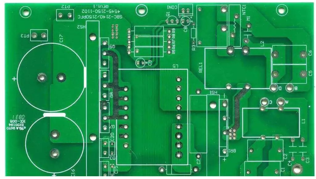
PCB and circuit anti-interference measures
Printed circuit board anti-interference design is closely related to the specific circuit. Next, we will only make some explanations of several common measurement methods PCB anti-interference design.

Power line design
Depending on the size of the printed circuit board current, try to add new widths of power lines to reduce the loop resistance. At the same time, make the direction of the power and ground lines consistent with the direction of data transmission, which helps to enhance noise immunity.
The principles of ground line design are:
(1) Separate digital ground from analog ground. If both logic and linear circuits exist on the board, they should be separated as much as possible. Low-frequency circuit grounding should be as far as possible in a single point of parallel grounding. When practical wiring is difficult, they can be partially connected in series and then connected to ground in parallel. High-frequency circuits should be grounded in series at multiple points, the grounding wire should be shorted and leased, and a grid-like large-area grounding foil should be used as much as possible around the high-frequency components.
(2) Ground wires should be as thick as possible. If a very tight line is used for the ground wire, the ground potential will vary with the current, which will reduce noise immunity. Therefore, the ground wire should be thickened so that it can pass three times the allowable current through the printed board. If possible, the ground wire should be 2 to 3 mm or larger.
(3) The ground wire forms a closed loop. For printed circuit boards consisting only of digital circuits, most of their grounding circuits are arranged in loops to improve noise immunity.
Decoupling Capacitor Configuration
One of the traditional methods of PCB design is to configure appropriate decoupling capacitors in each critical part of the printed board. The general principles of decoupling capacitor configuration are:
(1) Connect a 10-100uf electrolytic capacitor at the power input. If possible, it is best to connect to 100uF or higher.
(2) In principle, each IC chip should be equipped with a 0.01pF ceramic capacitor. If the clearance of the printed board is not sufficient, 1-10pF capacitors can be configured for every 4-8 chips.
(3) Decoupling capacitors should be connected directly between the power and ground lines of the chip for devices with weak noise immunity and large power changes during shutdown, such as RAM and ROM storage devices.
(4) Capacitor leads should not be too long, especially high-frequency bypass capacitors.
Eliminate electromagnetic interference methods PCB design
(1) Reduce loops: each loop is equivalent to an antenna, so we need to minimize the number of loops, the area of the loop and the antenna effect of the loop. Make sure that the signal has only one loop at any two points, avoid artificial loops, and try to use the power layer.
(2) Filtering: Filtering can be used to minimize electromagnetic interference on the power and signal lines. There are 3 methods: decoupling capacitors, EMI filters, and magnetic components.
(3) Masking.
(4) Minimize the speed of high-frequency equipment.
(5) New PCB board dielectric constant can prevent high-frequency parts, such as transmission lines close to the PCB board, from radiating outward; new PCB board thickness and minimizing the thickness of microstrip lines can prevent electromagnetic lines from overflowing and radiation.