Silicon chip is silicon wafers used to make silicon semiconductor circuits, the original material of which is silicon. High purity polycrystalline silicon is dissolved and doped into silicon crystal seeds, which are then slowly pulled out to form cylindrical single crystal silicon. Silicon crystal rods are ground, polished, and sliced to form silicon wafers, also known as silicon wafers.
Silicon wafers, also known as wafers in English, are thin sheets of high-purity crystalline silicon. Silicon wafers are particularly useful as a substrate for chips and in the manufacture of electronic circuits. Silicon ranks as the seventh most common element in the entire universe and the second most common element on Earth. Some common materials containing silicon include sand and quartz. Silicon is one of the main elements in building materials such as bricks, cement and glass. Silicon is currently the most widely used semiconductor in semiconductor technology.
Although silicon chips may look like metal, they are not exactly metal. Metals are good conductors of electricity due to the easy movement of “free electrons” between atoms, and electricity is the movement of electrons. On the other hand, a pure silicon crystal is almost an insulator; very little current is allowed to pass through it. However, the ability of silicon to conduct electricity can be changed by doping the wafer.
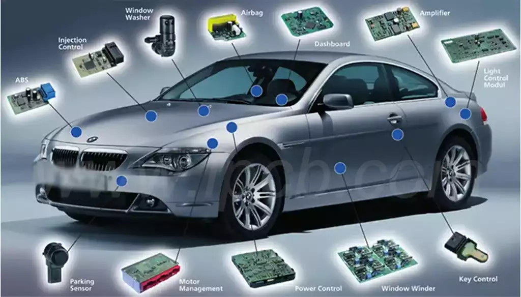
Silicon wafers are about 1 millimeter (mm) thick or less, and round silicon wafers are generally divided into 6-inch (150mm), 8-inch (200mm), 12-inch (300mm), and 18-inch (450mm) sizes according to diameter. In the silicon wafer substrate can be made into a variety of circuit components structure, and finally cut the wafer package into a very small integrated circuit chip with a specific electrical function, used in automobiles, computers, servers, as small as the charger, Bluetooth headset, memory cards, as long as there is a storage and logic calculation function of the chip have come from the silicon wafer figure.
The manufacturing process of silicon wafers:
Silica (by reduction) -> Silicon metal (by purification) -> Polycrystalline silicon (by heating and melting in the crucible) -> Molten silicon (by straight drawing method of long crystal) -> Monocrystalline silicon rods (by wire knife cutting) -> Silicon wafers (by chemical-mechanical milling) -> Polished wafers (by heat treatment) -> Annealed wafers (by epitaxial growth) -> Epitaxial wafers (by a variety of processes in conjunction with) -> Manufacture of various integrated circuits or discrete devices
Silicon wafers: remove the head and tail of the monocrystalline silicon rods, leaving the middle part of the rods of silicon blanks, and then cut and processed to obtain the silicon wafer.
Polished wafer: the cut silicon wafer after chamfering, grinding to make it single-sided or double-sided mirror state.
Annealed wafer: For part of the silicon wafer in the polished but also into the diffusion furnace for heat treatment to ensure that the surface of the silicon wafer to become a defect-free layer, that is, annealed wafer.
Epitaxial wafer: on a single-crystal substrate to make the growth of a single-crystal film with the same crystalline phase and substrate. The epitaxial layer can be homogeneous epitaxial or heterogeneous epitaxial.
Wafer: usually cut silicon wafers are called bare wafers, the further completion of a variety of circuits on the silicon wafer after the production process is called a wafer.
Chip: In the end-use market, integrated circuits/ICs are usually referred to as chips, but in the semiconductor generation process, a chip usually refers to an individual Die/bare chip cut from a wafer.
Semiconductor discrete device: refers to a single device that does not need to be integrated with other devices, a single device exists as an entity to perform a specific function, for example, including but not limited to: diodes, transistors, thyristors, MOSFETs, IGBTs.
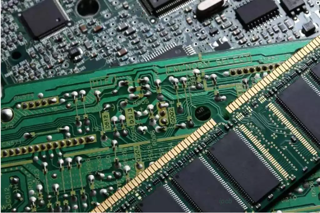
Integrated Circuit/IC: An electronic device that integrates a large number of miniature electronic components on a single silicon wafer to process and store electronic parts for various functions.
Module: A circuit unit in which multiple components are connected together by means of a carrier board or circuit board. A power module is usually a circuit unit that integrates multiple power devices through a carrier board in a single package, while some small-signal/low-power modules may not have a hermetically sealed enclosure.
Technical difficulties in silicon wafer manufacturing
Silicon wafer manufacturing is a high-precision, high-tech manufacturing process, requiring precision manufacturing equipment and perfect manufacturing process, the requirements for manufacturing technology and process control are very high.
- Wafer growth technology
Wafer growth technology is one of the important links in the manufacture of silicon chip, at present, the main use of Czochralski (CZ) method of growth of monocrystalline silicon, silane vapor deposition (SiH4) growth of polysilicon. - Wafer cutting technology
Silicon wafers need to be cut into a certain thickness after growth, but the cutting process needs to overcome a lot of technical difficulties, because silicon wafers have a high degree of brittleness, the stability of the cutting quality has a decisive impact on the precision of chip manufacturing. - Surface treatment technology
The purity, flatness, absence of defects, chemical activity and other characteristics of the surface of silicon wafers have an important impact on the manufacturing accuracy of the chip and the performance of the end product.
The role of silicon wafers in chip manufacturing
1.Chip engraving
Chip etching is one of the important steps in the production of chips. Silicon wafers, as the carrier of chip etching, have excellent mechanical stability and high surface flatness, and are capable of carrying a variety of graphics of semiconductor devices, as well as a variety of graphic processing and production processes.
2.Chemical Processing
Chemical processing is one of the important steps in chip manufacturing. Through the chemical reaction on the surface of silicon wafers, an oxide layer, nitride layer, etc. can be formed on the surface to achieve a variety of purposes such as protection, modification and creation of new surface structures.
3.Photolithography
Photolithography is an important process in chip manufacturing, using photolithography to project the pattern on the mask through the ultraviolet light on the silicon wafer to the photoresist or silicon oxide photoresist photoresist, so that the chip in this area to leave the chip on the graphic or deformation, so as to achieve the purpose of chip manufacturing.
Silicon chip, as the core foundation of semiconductor technology, not only supports the rapid development of the modern electronics industry, but also a key force in promoting human scientific and technological progress. From silica to high-purity monocrystalline silicon rods, and then through the precision processing of silicon wafers, every step of the process has condensed the wisdom and efforts of scientific and technological personnel. Silicon wafers with high transparency, high stability, easy processing and other characteristics, making it an ideal material for manufacturing chips.