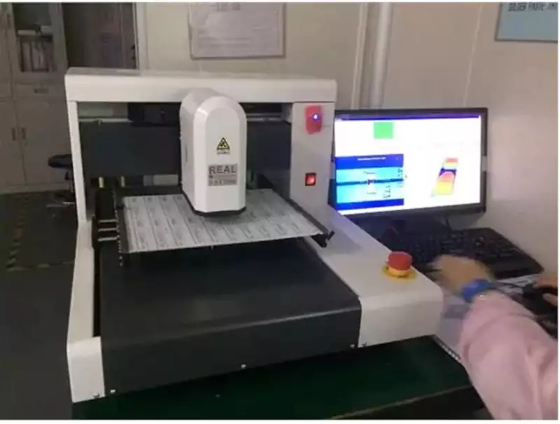
What is Solder Paste Inspection?SPI, or Solder Paste Inspection, is a technique for inspecting the solder paste printing aspect of SMT processing. It evaluates the printing quality of solder paste by measuring the volume, area, height and other parameters of the paste on the circuit board, so that problems such as insufficient, excessive or offset solder paste can be detected in a timely manner.
Solder paste printing is one of the key links in SMT processing, and its quality directly affects the subsequent component placement and soldering results. If the solder paste is poorly printed, it may lead to component placement is not solid, poor soldering and other consequences. Therefore, SPI technology is equally important in ensuring the quality of SMT processing.
Common solder paste inspection defects, mainly more tin, less tin, offset, even tin, tin high, and so on. Paste position offset or excessive amount of paste can easily cause the solder joints to be connected to each other, forming a short circuit after reflow soldering; less tin and lack of tin can easily lead to false soldering.
The process of solder paste inspection that is the quantitative inspection of solder joints, and through the statistical process control tools, predict the process trend of solder paste printing, before the defects generated in a timely manner to adjust the printing parameters, not only to improve the one-time pass rate of the printed product, but also reduce the cost of rework.
In addition, combined with the AOI automatic optical inspector, SPI has become an indispensable part of the lean assembly process.
SPI: The function is to detect whether the height, volume, area, short circuit and offset are qualified after solder paste printing. Placing SPI after solder paste printing can screen out the PCB with poor solder paste printing before placement, which can improve the pass rate after reflow soldering and save cost.
AOI: It works on the principle that the high-definition CCD camera automatically scans the pcba products, collects images and compares them with the database, detects and marks the defective places. The role is to detect the presence of defective PCB solder joints after reflow soldering, can be more accurate and rapid detection of defective, improve production quality.
SPI is used after the printing machine, for the quality inspection of solder printing and printing process verification and control.SPI plays a considerable role in the whole SMT. AOI is divided into two kinds of furnace and furnace, the former for device placement detection, the latter for the detection of solder joints.
Difference between AOI and SPI
01.Different inspection objects
AOI technology is mainly for the SMT process components and solder joints for inspection, while SPI technology is focused on the solder paste printing link quality assessment. This is the most obvious difference between the two.
- Different inspection principles
AOI technology uses optical principles to analyze the image on the board, through image processing algorithms to identify defects. SPI technology, on the other hand, evaluates the printing quality of solder paste by measuring the parameters of the paste on the circuit board, such as volume, area, height, and so on. - Inspection timing is different
In the SMT process, AOI technology is usually in the component placement and soldering is completed after the inspection to ensure the quality of soldering and component placement accuracy. SPI technology in the solder paste printing is completed immediately after the inspection, in order to timely detection and treatment of poor solder paste printing problems. - Different impact on productivity
Although AOI and SPI technology can help improve the quality of SMT processing,but their impact on productivity is slightly different.AOI technology can be completed after the completion of the soldering one-time detection of multiple soldering points,faster detection speed, the impact on productivity is relatively small. SPI technology needs to be detected immediately after the completion of solder paste printing,if the detection of defective products,you may need to stop to adjust the printing parameters or cleaning circuit boards, so the impact on production efficiency is relatively large.
How to choose the right inspection technology?
When selecting AOI and SPI technology, the following factors need to be considered:
- Production requirements:According to the actual situation of the production line and product requirements, to determine the items to be inspected and accuracy requirements.
- Cost budget:The price and maintenance cost of AOI and SPI equipment may vary and need to be weighed against the budget.
- Technology level:Consider the skill level of the operator and the cost of training, choose equipment that is easy to operate and maintain.
Generally speaking, for high-demand, high-volume SMT processing line, it is recommended to use both AOI and SPI technology to ensure production quality and efficiency. And for small batch, low requirement production line, you can choose one of the technologies for inspection according to the actual situation.
In the field of SMT processing, the quality of solder paste inspectian and component placement soldering directly determines the performance and reliability of the product. When choosing SPI and AOI inspection technology, we need to comprehensively consider factors such as production demand, cost budget and technical level. Only by choosing the right technology can we maximize its role in SMT processing, improve production efficiency, reduce the rate of defective products, thus creating greater value for the enterprise.