AI server PCBs are high-performance boards specifically engineered to meet the demanding requirements of artificial intelligence and machine learning workloads. Serving as the server’s central nervous system, they interconnect critical components such as GPUs, CPUs, high-bandwidth memory (HBM), and high-speed network interfaces, facilitating the massive data exchange essential for complex computations. Unlike standard server PCBs, AI server circuit boards must withstand significantly higher data rates, power densities, and thermal loads, representing the pinnacle of modern electronic manufacturing.
The core function of AI server PCBs lies in providing stable, reliable, and ultra-high-speed foundational support for the hardware driving artificial intelligence. As AI models grow increasingly complex, the demand for parallel processing across multiple GPUs and processors becomes ever more critical. This necessitates PCB architectures capable of maintaining flawless signal integrity at data transfer speeds exceeding 32Gbps, or even 64Gbps. According to iPCB® experts, such circuit boards must support massive interconnect bandwidth, which is vital for preventing data bottlenecks that could compromise the performance of powerful AI chips.
AI server PCBs exhibit several key differences from conventional PCBs: their design focuses on minimising signal loss, managing extreme thermal conditions, and accommodating ultra-high-density component placement (such as fine-pitch ball grid array BGAs). These compounding demands continually push the boundaries of materials science and manufacturing processes, requiring designers to adopt holistic solutions that balance electrical performance, thermal stability, and mechanical reliability.
Core characteristics of AI server PCBs include:
High-speed signal integrity: AI server PCBs must support interfaces like PCIe Gen5/6 and high-speed memory buses to achieve extremely rapid data transfer rates. This necessitates precise impedance control (typically within ±5% tolerance), trace length matching to prevent data skew, and strategies to mitigate crosstalk between adjacent signal lines.
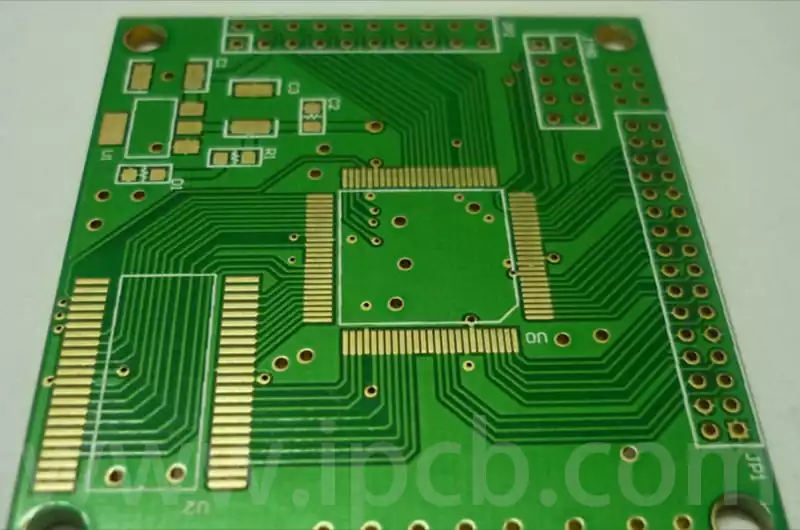
High-Density Interconnect (HDI): To connect thousands of pins on modern GPUs and ASIC chips, these boards employ advanced HDI techniques. This includes microvias, blind/buried vias, and multilayer lamination processes to achieve high-density routing while ensuring signal path integrity.
Advanced Thermal Management: AI processors generate hundreds of watts of heat within compact footprints. The PCB itself functions as a critical thermal component, utilising features like thermal vias, embedded copper pads, and thick copper layers to dissipate heat from components towards heat sinks or liquid cooling systems.
Superior Power Integrity: AI chips exhibit volatile current demands, prone to voltage sags that threaten system stability. AI server PCBs employ robust, low-impedance power distribution networks (PDNs) extensively populated with decoupling capacitors, guaranteeing clean, stable power delivery under all operating conditions.
Hardware Dissection of AI Server PCBs
The internal architecture of an AI server constitutes a complex ecosystem where specialised PCBs operate in concert. Unlike standard servers where the CPU motherboard holds absolute centrality, the value and performance of AI servers are primarily concentrated in GPU-centric components. Through hardware teardown analysis of systems like the NVIDIA DGX A100, its PCB components can be functionally categorised into GPU motherboard assemblies, CPU motherboard assemblies, and various auxiliary modules.
As the core of AI servers, the GPU motherboard assembly commands the largest share of total PCB value.This component is not a single circuit board but comprises multiple interconnected high-performance PCBs designed to support the GPU and its high-speed communication links. While the CPU motherboard component remains crucial, it primarily serves an auxiliary role, managing system resources, I/O, and general-purpose computing tasks. Despite its high design complexity, it generally resembles traditional high-performance server motherboards.
The intricate interplay between these components is fundamental to enabling the massive parallel processing capabilities of AI servers. The GPU component shoulders the primary responsibility for AI model training and inference, while the CPU component coordinates data flow and system management.
Key Design Challenges: Signal Integrity, Power and Thermal Management
Designing a fully functional and reliable AI server PCB requires overcoming three critical engineering challenges: maintaining signal integrity in an ultra-high-speed environment, delivering stable power through complex power delivery networks, and effectively managing the intense heat generated by high-performance components. These three pillars – signal, power and thermal management – are intertwined and demand a holistic solution from the earliest stages of design. Failure in any single domain may result in performance degradation, data corruption, or even catastrophic hardware failure.
Signal integrity is paramount. When hundreds of differential pairs operate at speeds exceeding 28 Gbps, even minute PCB imperfections can cause data corruption. Designers must rigorously control impedance, ensure trace lengths are precisely matched to millimetre accuracy, and meticulously manage each signal’s return path to prevent reflections and crosstalk. Any discontinuity—such as layer transitions without properly stitched vias—can create antenna effects, radiating electromagnetic interference (EMI) and disrupting neighbouring signals.
The power distribution network (PDN) is equally vital. AI processors may consume hundreds of amperes and exhibit explosive transient currents, switching from low-power to high-power states within nanoseconds. The PDN must exhibit extremely low impedance (typically below 5 milliohms) to prevent voltage sags during these events. This is achieved through wide copper planes, strategically placed arrays of high-capacity, high-frequency decoupling capacitors near the processor, and meticulously laid-out multi-phase voltage regulator modules (VRMs).
Finally, thermal management presents a critical make-or-break challenge. Flagship GPUs can exceed 700 watts of power consumption, with junction temperatures rapidly surpassing 120°C without robust cooling. The PCB plays a pivotal role in this process. Designers incorporate arrays of thermal vias beneath heat-generating components to channel heat into internal copper layers or heat sinks on the board’s reverse side. In extreme cases, embedded copper plates or direct liquid cooling via cold plates become essential to maintain silicon temperatures within safe operating limits, thereby safeguarding performance and long-term reliability.
Engineers may address core challenges by adhering to the following checklist:
Signal Integrity: Employ low-loss dielectric materials. Maintain controlled impedance (e.g., 100 Ω for differential pairs). Ensure matched trace lengths for high-speed buses. Employ solid reference planes and avoid routing across partitioned zones.
Power Distribution Network (PDN): Pursue low impedance (<5 mΩ). Combine high-capacitance and high-frequency decoupling capacitors near loads. Utilise wide power planes with fill areas, avoiding sharp 90° corners. Simulate voltage sags and power rail breakdown scenarios.
Thermal Management: Employ thermal simulation software (CFD) during initial design stages. Position thermal via arrays beneath high-power components. Consider thick copper layers or embedded copper plates for thermal spreading. Plan mechanical cooling solutions such as heatsinks, vapour chambers, or liquid-cooled cold plates.
Advanced Materials and Manufacturing Technologies for Artificial Intelligence Circuit Boards
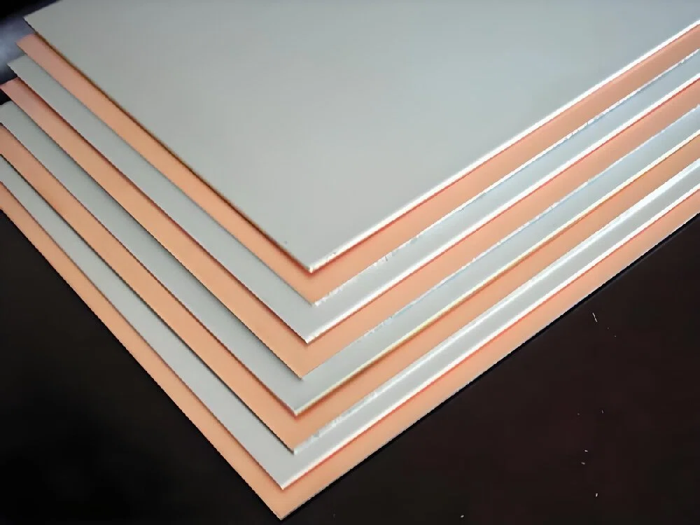
The extreme performance demands of AI server PCBs push conventional circuit board manufacturing to its limits, necessitating the adoption of advanced materials and precision manufacturing processes. Whilst standard FR-4 materials remain the mainstay for most electronic devices, they fail to meet the high-frequency signal transmission and intense thermal load requirements of AI hardware. Consequently, designers must turn to specialised laminates—materials that, though more costly and demanding to manufacture, deliver lower signal loss and superior thermal stability.
Material selection forms the foundational decision in AI server PCB design. Critical electrical properties include dielectric constant (Dk or εr) and loss factor (Df or tan δ, the tangent of loss). For multi-gigabit signals, materials with low, stable dielectric constants and extremely low loss factors are essential to minimise signal attenuation in long traces. Materials such as Megtron 6 or Isola I-Speed are widely adopted for meeting interface requirements like PCIe 5.0/6.0 and 56+ Gbps Ethernet. These low-loss hydrocarbon or ceramic-filled laminates ensure signals arrive at the destination with clear eye patterns, critical for achieving low bit error rates.
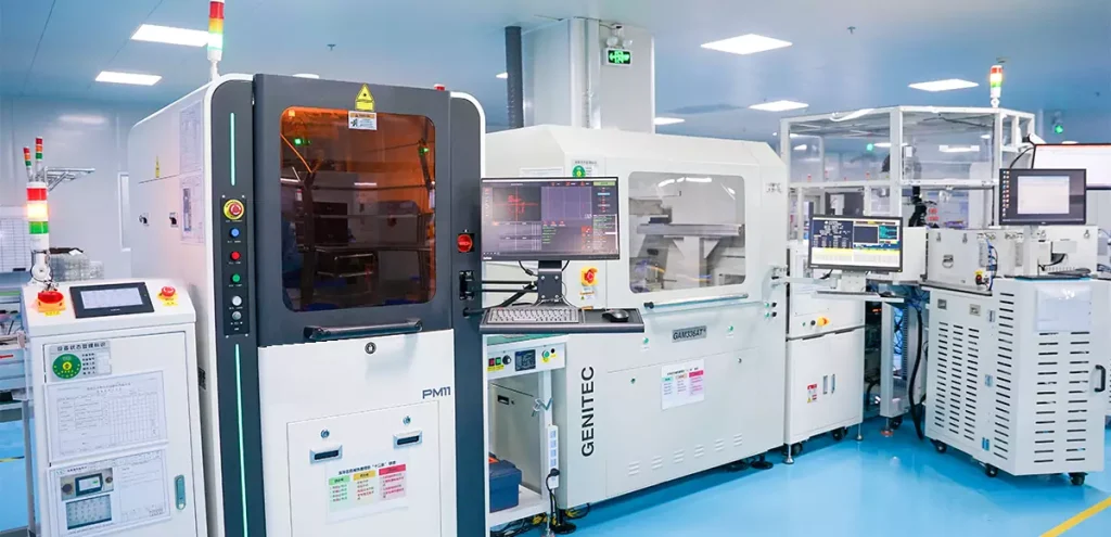
The manufacturing processes for these boards are equally sophisticated. AI server PCBs typically employ 20 layers or more, featuring complex high-density interconnect (HDI) architectures. Such designs rely on sequential lamination—a phased stacking process enabling blind and buried via fabrication. This technique supports ultra-dense routing layouts, allowing designers to navigate thousands of connection points from large BGAs without compromising signal integrity. The precision required for drilling micro-laser vias and the process demands for ensuring layer-to-layer alignment present significant manufacturing challenges, achievable only by specialist manufacturers.
Artificial intelligence is also reshaping the design process itself. While AI cannot yet independently complete complex PCB designs from scratch, it is becoming an indispensable tool for engineers. AI-driven software assists in optimising component placement, automating routing design, and conducting signal integrity analysis, effectively addressing intricate design challenges. This synergy between AI software and human engineering expertise enables the creation of more optimised, reliable circuit boards within shorter timeframes.
Key considerations for AI-driven PCB manufacturing include:
Material compatibility: Ensuring selected low-loss materials align with manufacturer processes, such as employing plasma decontamination for via cleaning.
Lamination and stack-up processes: Planning complex multi-stage lamination cycles for HDI boards requires precise temperature and pressure control to prevent delamination or warping.
Drilling and plating accuracy: Employing laser drilling for microvias and ensuring copper plating uniformity (particularly for high aspect ratio through-holes) guarantees connection reliability.
Back-drilling process: Remove unused portions (stubs) of vias on high-speed signal paths to reduce signal reflection and enhance overall signal integrity.
Quality assurance: Employ comprehensive testing methods, including automated optical inspection (AOI) and X-ray inspection, to verify internal layer structures and BGA solder joint integrity.
As the pinnacle of modern electronic engineering, AI server PCBs push the boundaries of computational power with every advancement in design, materials, and manufacturing processes. From the meticulous pursuit of signal integrity to the extreme challenges of thermal management, and from the innovative application of advanced materials to the deep integration of AI-assisted design, developments in this field not only demonstrate the ingenuity of engineering but also herald the boundless potential of future intelligent hardware.