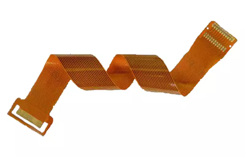
Flexible printed circuits (FPC), owing to their pliable nature, have found exceptionally widespread application within the electronics sector, proving particularly well-suited to scenarios where space is at a premium.
As electronic devices continue their trajectory towards miniaturisation, the scope of FPC utilisation grows ever broader. In the assembly stages of numerous consumer products, constrained by spatial limitations, surface-mount device (SMD) components are frequently mounted onto flexible pcb to complete the assembly of the entire unit. Today, FPCs have become indispensable components in digital products such as calculators, mobile phones, digital cameras, and camcorders. Meanwhile, surface mount technology (SMT) for SMDs has been fully utilised and further developed on flexible pcb board.
Pre-treatment of Flexible PCB
Owing to the flexible nature and hygroscopic properties of flexible PCBs, pre-baking treatment is mandatory prior to SMT production. This process aims to eliminate absorbed moisture. Without proper pre-treatment, moisture absorbed by the flexible PCBs during reflow soldering will rapidly vaporise under high temperatures, potentially causing delamination or bubbling.
Pre-baking conditions are typically set at 80–100°C for 4–8 hours. In exceptional cases, temperatures may exceed 125°C, though baking duration must be correspondingly reduced. Prior to baking, small-scale trials must confirm the FPC’s tolerance to the specified baking temperature. Following baking, inspect the FPC for defects such as discolouration, deformation, or warping. Only after passing IPQC sampling checks may it proceed to the production line.
Given the insufficient rigidity and soft texture of flexible pcb boards, dedicated carrier boards are essential for securing and transporting them. Without these, SMT processes—including printing, component placement, and reflow soldering—cannot be successfully completed.
Fabrication of Dedicated Carrier Boards
Dedicated carrier boards play a critical role in fpc smt production. They not only secure and transport flexible pcbboards but also ensure the smooth execution of SMT processes. Based on the circuit board CAD files, the hole positioning data of the flexible pcb is extracted to manufacture high-precision FPC positioning templates and dedicated carrier boards. The diameter of the locating pins on the template must precisely match the aperture of the locating holes on both the carrier plate and the FPC to guarantee accurate positioning. As flexible pcbs thickness may vary due to circuit protection or design requirements, the interface between the carrier plate and FPC necessitates machining, grinding, or slot-cutting according to actual conditions. This ensures the FPC remains flat during printing and placement.
FPC Fixing Method
Prior to commencing the SMT process, the primary task is to securely fix the FPC to the carrier board. It is important to note that the storage time from when the flexible pcb is fixed until the final printing, placement, and soldering processes should be minimised as much as possible. Carrier boards can be categorised into two types: those with locating pins and those without. For carrier boards without locating pins, they must be used in conjunction with a locating template equipped with locating pins. During use, first position the carrier board over the template’s locating pins, ensuring the pins pass through the carrier board’s locating holes. Subsequently, individually position each flexible pcb over the exposed locating pins and secure them using adhesive tape. Subsequently, separate the carrier board from the FPC positioning template to proceed with subsequent printing, placement, and soldering operations. Should the carrier board incorporate its own locating pins, the flexible pcb may be directly fitted onto the carrier board’s spring-loaded locating pins, again securing it with adhesive tape.
During the printing process, the spring-loaded locating pins are fully depressed into the carrier board by the stencil, thus having no impact whatsoever on the printing outcome.
Additionally, two common FPC securing methods exist. One involves using single-sided adhesive tape to firmly secure all four edges of the FPC to the carrier board, preventing displacement or warping. When selecting adhesive tape, ensure its viscosity is moderate to facilitate easy removal after reflow soldering without leaving adhesive residue on the FPC. Utilising an automatic tape dispenser enables rapid cutting of uniformly sized tape lengths, significantly enhancing efficiency while reducing costs and waste.
An alternative approach involves using double-sided adhesive tape. First, apply heat-resistant double-sided tape to the carrier board, achieving a similar effect to silicone pads. Subsequently, affix the flexible pcb to the carrier board. It is crucial to note that the adhesive strength should not be excessively high to prevent tearing the FPC during removal after reflow soldering.
FPC Printing and Placement Process
FPCs impose stringent requirements on high-precision solder paste printing and placement. While they do not impose specific composition requirements on the solder paste, the primary focus lies on the particle size of the solder balls and the metal content. However, the printing performance of the solder paste must be exceptionally high. The paste requires excellent thixotropy to facilitate printing and release from the stencil, while also adhering firmly to the flexible pcb surface. This prevents defects such as poor release, stencil aperture blockage, or post-printing collapse.
Given potential micro-gaps between the FPC and carrier board, precise equipment parameter settings are crucial for optimal printing results. Maintaining cleanliness at the printing station is paramount to prevent FPC contamination. Operators must wear finger cots and regularly wipe the stencil to avoid solder paste fouling the FPC’s gold fingers and plated-through pads.
Depending on product characteristics, component count, and placement efficiency requirements, either medium-speed or high-speed placement machines may be selected. As the flexible pcb is fixed to the carrier board but lacks the flatness of rigid PCBs, precise adjustment of the placement machine’s nozzle descent height and air pressure is essential.
FPC Reflow Process
To ensure uniform temperature distribution across the flexible pcb, a forced convection infrared reflow oven is recommended. This equipment enables more balanced temperature distribution across the flexible pcb, thereby reducing the risk of soldering defects.
During reflow, the heat absorption rate and thermal capacity of the carrier board and flexible pcb components vary due to the board’s thermal properties and the diversity of FPC components. Consequently, meticulous configuration of the reflow oven’s temperature profile is critical for ensuring soldering quality.
FPC Inspection and De-panelisation Process
Removed FPCs should undergo visual inspection under magnification of at least 5x, focusing on residual adhesive, discolouration, and issues such as solder contamination or lack of solder balls on gold fingers. Due to potential surface irregularities leading to high AOI misjudgement rates, flexible pcbs are generally unsuitable for AOI inspection. However, with specialised test fixtures, flexible pcb can successfully pass ICT and FCT testing.
For flexible pcb with multiple interconnected panels, separation may be required prior to ICT or FCT testing. While blades or scissors can achieve separation, these methods yield lower efficiency, poorer quality, and higher scrap rates. For high-volume production of irregularly shaped flexible pcb, it is advisable to fabricate specialised flexible pcb punching dies. Utilising punching for separation significantly enhances operational efficiency while ensuring clean, aesthetically pleasing edges on the cut FPCs.
During flexible pcb production, SMD placement constitutes a critical stage where precise positioning and secure fixation are paramount. Appropriate carrier boards must be fabricated to guarantee effective fixation. Additionally, flexible pcb undergo multiple process steps including pre-baking, printing, component placement, and reflow soldering. Given the heightened complexity of SMT processes for flexible pcb compared to rigid PCBs, meticulous parameter setting and rigorous production process management prove particularly crucial. Operators must strictly adhere to Standard Operating Procedures (SOPs), while line engineers and In-Process Quality Control (IPQC) personnel should intensify patrol inspections to promptly identify and address production line anomalies. This approach effectively maintains the FPC SMT production line’s defect rate at a low level.