Make your own pcb board is a complex and specialized process that involves multiple steps and considerations. The following is a general design process:
- Pre-Preparation
Before proceeding with the PCB design, it is important to prepare the required component libraries and schematics. This includes creating or acquiring the appropriate SCH component libraries and PCB component package libraries. PCB component package libraries usually need to be built based on the actual size of the selected device, while schematic SCH component libraries are relatively flexible, but care needs to be taken to define the pin attributes and their correspondence with the PCB component package libraries.
2.PCB Structure Design
According to the size of the circuit board and mechanical positioning requirements, in the PCB design environment to draw the circuit board frame, and in the appropriate location to place connectors, switches and keys, screw holes and assembly holes. At the same time, we should give full consideration to the wiring area and the division of non-wiring area to ensure the rationality and feasibility of the design.
3.PCB layout design
Layout design is a variety of devices in accordance with the design requirements placed in the PCB board frame process. First of all, in the schematic tool to generate the network table, and then in the PCB design software to import the network table. After successful import, all devices will appear in the software in the form of flying wires prompted to connect, then you can start the layout design.PCB layout design is a key link in PCB design, the designer’s circuit knowledge and experience requirements are high. Elementary designers can start with small modules or simple tasks to gradually accumulate experience.
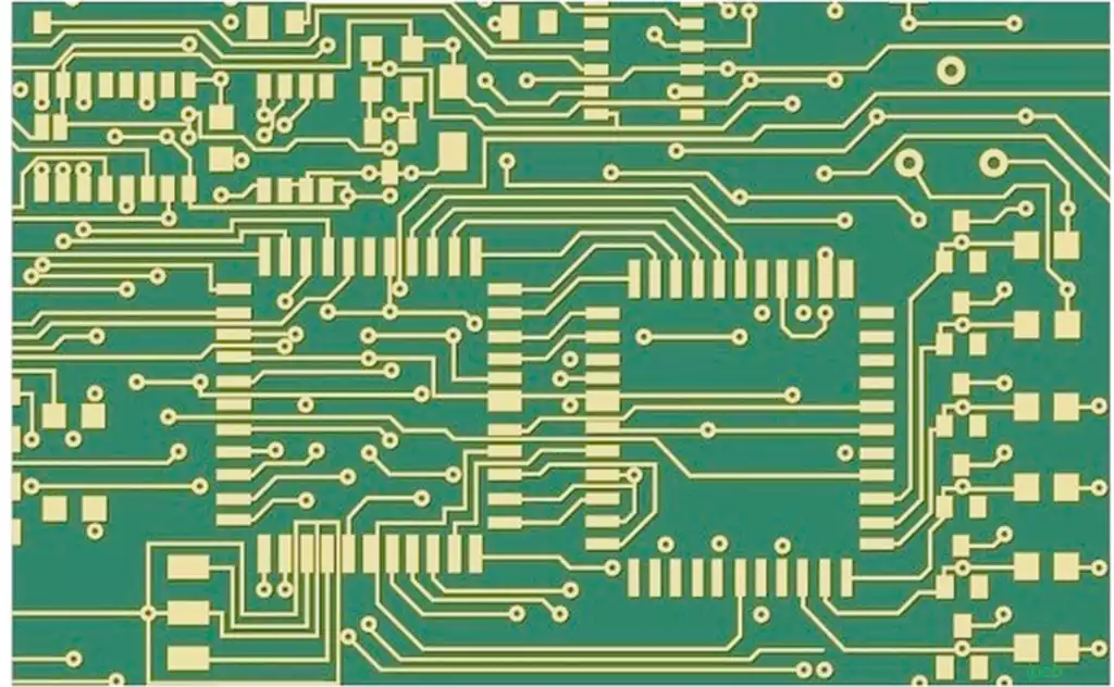
4.PCB wiring design
Cabling design is the largest part of the PCB design workload, the performance of the PCB board has a direct impact. The three levels of wiring design include: first of all, to ensure line connectivity, which is the basic requirements of PCB design; secondly, to meet the demand for electrical performance, to ensure that the function of the PCB board is normal; and finally, the pursuit of wiring neat and beautiful, easy to change the board later to optimize and test maintenance.
- Wiring optimization and silkscreen placement
PCB design is a continuous improvement process, wiring optimization is an important part of it. Optimization of wiring usually takes twice as long as the initial wiring. After completing the wiring optimization, post-processing is also required, including adjusting the position and direction of the silkscreen logo to ensure that the top and bottom silkscreens are not confused. - Network DRC Inspection and Structural Inspection
Quality control is an integral part of the PCB design process, which usually includes design self-inspection, mutual inspection, expert review and special inspection. Network DRC check and structure check is an important means to ensure that the PCB design meets the requirements of the schematic and structural elements. In addition, Valor check and DFM check are also required to focus on the compliance and manufacturability of the PCB design output back-end processing light drawing files.
7.PCB board making
Before the formal PCB processing board, circuit board designers need to communicate with the PCB supplier’s process engineers to confirm the parameters and requirements of the processing. This includes selecting the appropriate PCB board, adjust the line width and line spacing of the line layer, control impedance, adjust the thickness of the PCB stack, determine the surface treatment process, set the aperture tolerance and delivery standards. Through adequate communication and confirmation, you can ensure the quality and efficiency of PCB board making.
It should be noted that circuit board design is a highly specialized field that requires relevant electronic engineering knowledge and skills. If you are a beginner or do not have the relevant background, it is recommended to seek professional help or attend relevant training courses. Meanwhile, using professional circuit board design software can greatly improve design efficiency and accuracy.