Fiducials on pcb usually refer to markings or areas set at specific locations on a PCB for purposes such as element positioning, inspection and debugging. These fiducials not only play a guiding role in the production process of the PCB, but are also critical in subsequent testing and maintenance.
Classification:
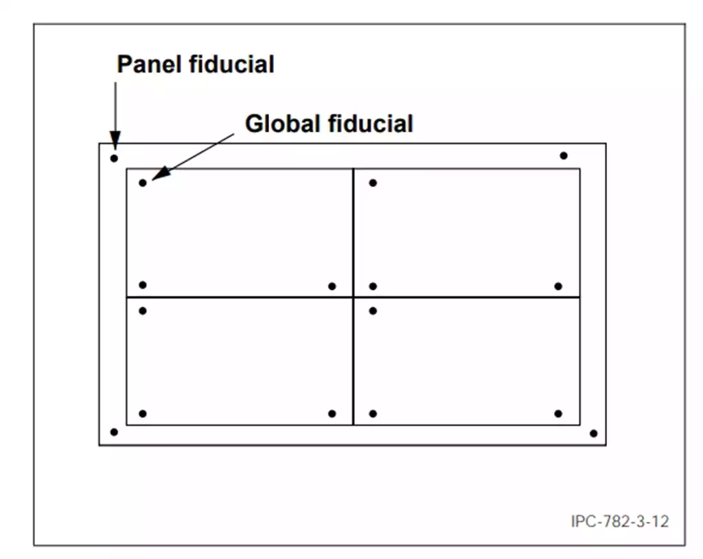
Reference points play a role in optical positioning during solder paste printing and component placement. According to its functional differences on the PCB, it can be divided into patchwork fiducials, single-board fiducials, and local fiducials (also known as device-level datum points).
In the process of piecing together the edge of the board and do not need to be pieced together on a single board, should be set up at least three L-shaped distribution of pcb fiducials, and these diagonal datum points relative to the centre of the position is asymmetric.
For both sides are fitted with components PCB board, each side should be equipped with the corresponding pcb fiducials.
For the need to put together a single board, if the conditions allow, should try to set the fiducials on pcb.However, if the space is limited and can not be placed datum point point, it can be omitted.
For QFP devices with lead centre distance less than or equal to 0.5mm and BGA devices with centre distance less than or equal to 0.8mm, etc., local pcb fiducials should be set up at diagonal positions near the diagonal of the centre points of these components to achieve accurate positioning.
When multiple SOP devices are close to each other (distance less than or equal to 100mm) to form an array, they can be considered as a whole and two local fiducials can be designed at their diagonal positions.
The role of fiducials on pcb:
Positioning correction core: fiducials serve as key positioning references for the placement machine (SMT), ensuring the precise layout of components on the PCB.
Enhanced placement accuracy: For components such as QFPs (quad flat packs), BGAs (ball grid arrays) and other components that require high-precision placement, fiducials significantly enhance placement accuracy.
Precise positioning of PCBs: In the PCB assembly process, marks play a role in accurately positioning each veneer, thus ensuring that the position of each veneer is accurate after the board is cut.
Inspection and repair assistance: fiducials are also used in automatic optical inspection (AOI) and X-ray inspection to assist in the detection of defects on the PCB and to assist in the repair of problems when they are found.

Mechanisms recognition:
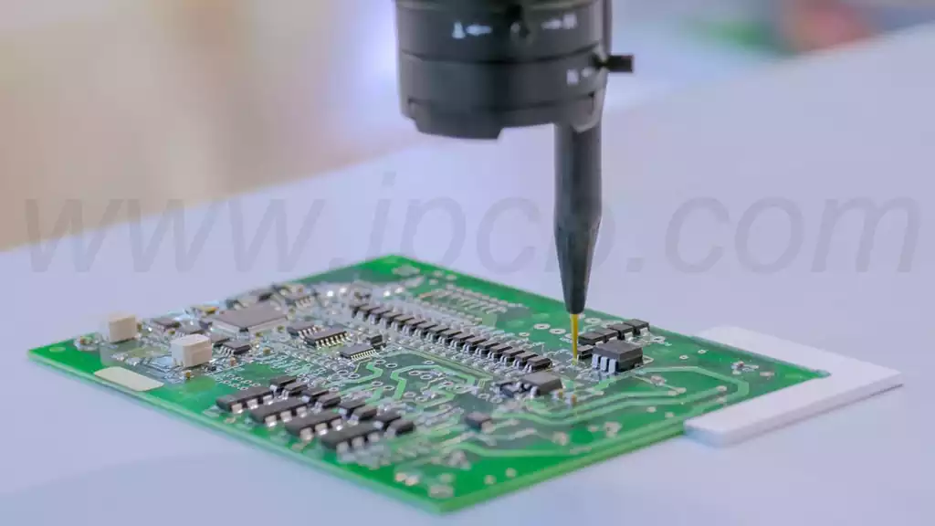
Optical system at the core: marks recognition mainly relies on the optical system built into the automatic placement machine or inspection equipment.
Image Capture and Algorithmic Processing: Optical sensors capture an image of the datum, and then use advanced image processing algorithms to accurately identify the location of the fiducials on pcb.
Position and Angle Calculation: Based on the identification of the fiducials, the system is able to calculate the relative position and angle of the PCB to ensure accurate positioning and alignment.
Design notes and dimensional specifications required:
The fiducials were designed as 1mm diameter solid circles in copper with a tinned surface. The fiducials on pcb were to be produced with good flatness, rounded and neat edges, and in a colour that contrasted with the surrounding background. The soldermask window is concentric with the fiducials, which is 3mm in diameter for panels and veneers and 1mm in diameter for localised marks.
On veneers,marks should be centred no less than 5mm from the edge of the board, while datums on process edges should be centred no less than 3mm from the edge of the board.
In order to ensure the recognition accuracy of the printing and placement process, the marks should be surrounded by avoiding the existence of pads, vias, test points, alignments, and silk-screen marking and other interfering factors, and at the same time need to be prevented from being cut by the V-CUT groove, which may lead to the machine not being able to accurately identify.
To improve the contrast between the marks and the substrate, copper foil can be laid under the fiducials. All marks on the same board should have the same inner background, i.e., the presence or absence of copper foil below the datum should be uniform.
For fiducials on single boards and patchwork boards, they should be designed as individual components; while local marks should be planned as part of the component package. Such a design facilitates the assignment of precise coordinate values to the datum points to achieve accurate positioning functions.
Guidelines for datum point selection: The selection of fiducials points has a direct impact on the placement efficiency and accuracy of the automatic mounter. When determining reference points, the machine model and its performance characteristics must be considered to ensure that the datum can be accurately and quickly identified. For example, some mounters may require datums of specific shapes or sizes to meet the specific needs of their optical identification systems.
Regarding the design of reference marks: During the design process, a set of established standards and guidelines must be adhered to in order to ensure these marks can be accurately recognised by automated SMT equipment and other automated machinery.
1:Selection of appropriate fiducials markings
Shape:marks are often chosen to be round, square or cross-shaped, and are designed to provide a highly recognisable and clear visual identity.
Size: Diameter is usually within the range of 1.0mm ± 0.2mm, but the exact size needs to be adjusted flexibly according to equipment requirements.
Material selection: Bare copper, tin or nickel plated are commonly used due to their good reflectivity and contrast.
2:Determine the layout and number of reference points
Layout strategy: fiducials should be placed at the diagonal position of the PCB to provide the most accurate positioning reference. For large or complex PCBs, additional marks may be required in the centre or other critical areas.
Quantity Requirements: At least one pair of fiducials points on the diagonal should be configured. For patchwork designs, at least one pair of datum points is also required for each single board.
3:Enhancing the contrast of fiducials
Background Clearance: Disturbing elements such as alignment, silkscreen or pads should be avoided around the datum to ensure clarity and contrast.
Colour contrast: The colour of the marks should contrast strongly with the background to facilitate accurate capture by the optical recognition system.
4:Setting up isolation areas for mark points
Copper digging treatment: Set up copper digging area around the mark point to reduce the interference of the neighbouring metal layer. Usually, the distance between the edge of the fiducials and the copper digging area is about 0.6mm.
5:Implementation of datum design in PCB design software
Placement of markers: In the PCB design software, select the appropriate fiducials markers from the package library and accurately place them at the specified location.
Copper digging area drawing: Use the copper digging tool to draw the isolation area around the mark point.
Double-sided board processing: for double-sided PCB, need to ensure that both sides are configured with mark points, and keep them aligned in the corresponding positions.
6:Verify the validity of the fiducials design
Design Review: Double check the size, position, contrast and isolation area of the fiducial to see if it meets the requirements.
Simulation test: Where conditions permit, conduct simulation tests using software to verify the recognisability of the datum points.
7:Manufacturing and Testing Phase
PCB Manufacturing: Submit the design files to the PCB manufacturer and ensure that they follow the design requirements of the marks point for manufacturing.
Datum Testing: Verify datum recognition performance on PCB samples to ensure they can be accurately read in real-world applications.
Caution:
Standards Compliance: Follow relevant standards such as IPC-SM-782A to understand the latest specifications and practice recommendations for fiducials.
Equipment compatibility: Consider the datum recognition capability of the SMT and AOI equipment used to ensure that the design meets the technical requirements of the equipment. When designing fiducial, all of the above factors need to be considered to ensure that they are used to maximum effect in automated production and inspection processes.
Fiducials on pcb design is the cornerstone of automated production and inspection accuracy. Through careful planning and strict implementation, we can guarantee the accurate identification and efficient function of the reference point, laying a solid foundation for high quality PCB manufacturing.


